
Worked examples
Each project here exists twice, generated from one description by
tools/make_examples.py:
| what it is | |
|---|---|
as-generated/ |
a deterministic negative control: deliberately incomplete title/part metadata and unreviewed layout details |
reviewed/ |
the rebuilt baseline accepted by its gate and project-specific contracts, with documented exceptions |
A repository full of good designs proves only that good designs pass. The pair is the evidence: that the rules catch what they claim to catch, and that fixing what they report converges.
Gate acceptance is not production sign-off. These are worked examples, not hardware-validated reference designs. In particular, the FPGA still has decoupling-distance exceptions; signal return paths, application-specific power/thermal budgets and EMC remain engineering review and measurement work.
./bin/eda.sh gate examples/buck-5v/reviewed     --policy examples/buck-5v/gate.toml --text
./bin/eda.sh gate examples/buck-5v/as-generated --policy examples/buck-5v/gate.toml --text
Regenerate the projects with:
docker run --rm -u $(id -u):$(id -g) -v "$PWD:/work" -w /work \
  -e PYTHONPATH=/work/src -e HOME=/tmp/eda-home \
  --entrypoint python3 eda-toolkit:9.0.9 tools/make_examples.py examples/
and the images below with
tools/example_images.py,
which runs the same two renders for every variant and writes them as JPEG:
docker run --rm -u $(id -u):$(id -g) -v "$PWD:/work" -w /work \
  -e PYTHONPATH=/work/src -e HOME=/tmp/eda-home \
  --entrypoint python3 eda-toolkit:9.0.9 tools/example_images.py examples/
The generator reads KiCad’s own symbol and footprint libraries, so these are the real parts, not simplified copies — which is why it runs inside the container.
After the five were built, the whole set was read the way an engineer would
read it — circuit theory, layout physics, readability — and every finding was
either turned into a rule, fixed in reviewed/, or answered with a reasoned
waiver in the project’s gate.toml. That pass, with what each finding became,
is REVIEW.md.
Three columns, not two
Each comparison below has three, and the leftmost is the honest one.
| column | what it is |
|---|---|
| first edition | the board as it came out of the generator the day it was written, before any finding had been read. Recovered from this repository’s own history — one git show per file, no editing — and rendered with today’s renderer so the only difference is the design |
| as-generated | what the generator produces now when told to skip the review. It is much better than the first edition, because twenty rounds of findings were built into the generator itself rather than patched into the output |
| reviewed | the same design with the review applied: what passes eda gate |
The middle column is the part that is easy to miss. A tool that only fixed its own output would leave the first column and the second identical; the distance between them is the review turned into code, and it arrives before anyone runs the gate. The distance between the second and the third is what the gate still had to catch on the day.
The first editions are ea93330 (buck-5v), e7ad2d7 (motor-driver),
b4d66f2 (pico-carrier), 3f796a7 (opamp-filter) and aee7401 (fpga-audio).
CI requires all five reviewed/ projects to pass and every as-generated/
negative control to fail for its intended missing-title and part-specification
defects. It checks that neither the schematic nor board stage was skipped.
The uploaded JSON verdicts and KiCad reports, not stale finding counts in this
historical walkthrough, are the authority for each revision.
What each of them still carries is a waiver, and a waiver here is a decision with the argument attached rather than a finding hidden. Package escape necks, board-only decoupling heuristics and deliberately exposed module rails remain visible there.
All five are two-layer boards, and that is a requirement rather than an
outcome. Layer count is the one board parameter that changes the price of a
prototype run outright, so a design that will not close on two layers grows a
few millimetres of FR4 before it grows a stack. The motor driver pays for that
with one waiver — route.return_path, measured at 12.8 mm and 10.4 mm against
a 10 mm limit, on two logic lanes crossing under the bridge outputs — and the
waiver says what a faster design should do instead. CI checks the two-layer
stack and that the ground pour on B.Cu is still mostly one piece.
Two rules keep the rest of it honest. layout.pour_edge_cut reports copper
that eats through the outermost millimetre of the ground pour: the rim is what
the board radiates into and what every edge-hugging track returns through, and
a mounting hole may interrupt it where a route may not. route.under_package
and route.via_under_package keep other nets’ tracks and vias out from under
the integrated circuits and connectors, where nothing can be probed, inspected
or reworked once the part is down. All three are warnings that the
ai-generated policy blocks on: a shipped board may carry them and be right,
a generated one has no argument for them.
All five carry what a board needs to be made as well as to work: the ground pour is filled by KiCad’s own filler against the board’s own rules, every through-hole land is relieved thermally, every track fillets into the land it enters, and each board has its M3 mounting holes and three fiducials for the assembly machine to align to. The holes clear the screw rather than the hole - a pan head on a washer is seven millimetres across, and a screw terminal’s wires want two more - which is why the count varies: four where the board has four free quarters, two on the boards whose left edge is a connector and a row of resistors. Three that hold a board flat beat four that hold one side of it. Rounds seventeen and eighteen in REVIEW.md are where that came from, and what it cost.
When these were made, and by what
Both variants carry it in their title block, in the comment fields, on the schematic and on the board:
(comment 1 "generated 2026-09-05 by Claude Code")
(comment 2 "from tools/make_examples.py in sabas0ba/kicad_skills")
It matters most on as-generated. That variant is a record of what a generator
of this vintage actually produced, and the point of keeping it is to be able to
say later how much has changed — which needs a date on it. The stamp is frozen
in GENERATED_ON / GENERATED_BY at the top of the generator rather than read
from the clock, so regenerating an unchanged design still produces an unchanged
file; bump them when you regenerate, or pass --generated-on / --generated-by.
The design’s own title, date, rev and company are a separate thing and
stay empty on as-generated — a generator that leaves them blank is one of the
findings, and the stamp deliberately does not paper over it.
buck-5v — 12 V to 5 V at 2 A
LM2596S-5, catch diode, output inductor, screw terminals in and out, and a fuse and a TVS between the input terminal and everything else.
Under KiCad’s own ERC and DRC, and the ai-generated policy:
| verdict | schematic (e/w/i) | board (e/w/i) | |
|---|---|---|---|
reviewed |
PASS, 1 finding waived | 0 / 0 / 0 | 0 / 0 / 5 |
as-generated |
FAIL, blockers retained | — | — |
| first edition | FAIL, 45 blocking | — | — |
The three, side by side
Everything below is this repository’s own output — eda sch render and
eda pcb render, run on the three variants and cropped. Nothing is drawn by hand.
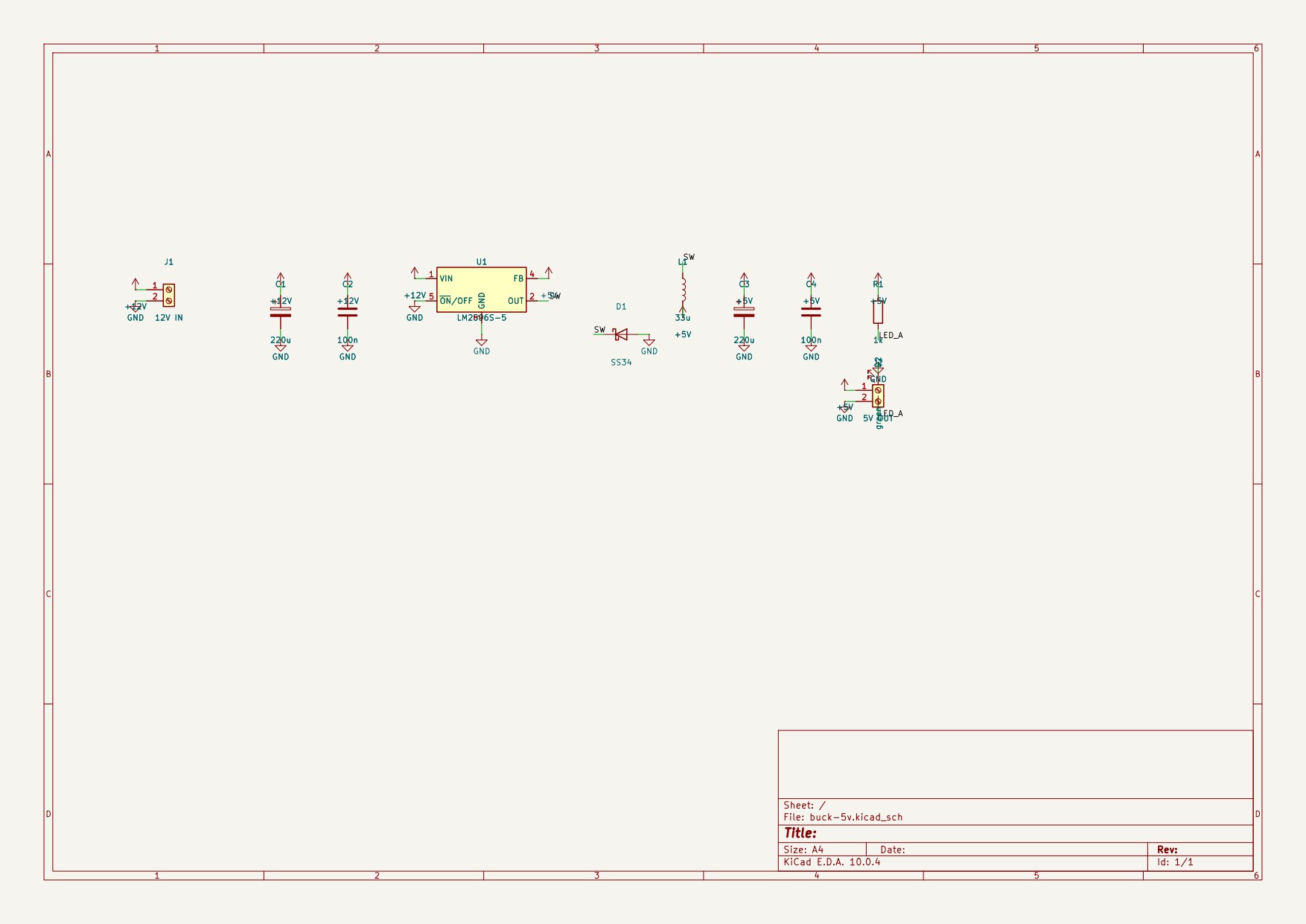
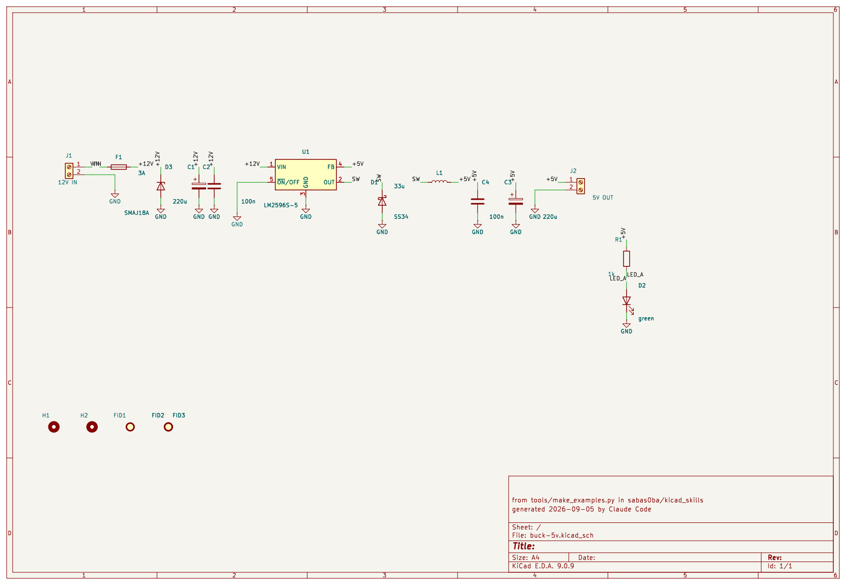
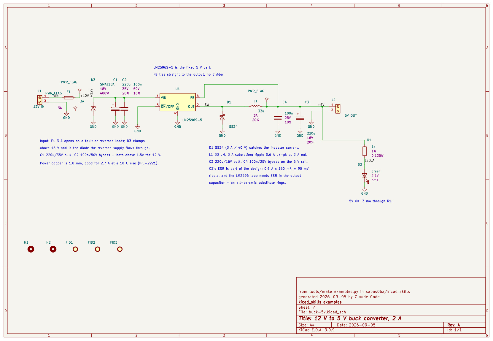
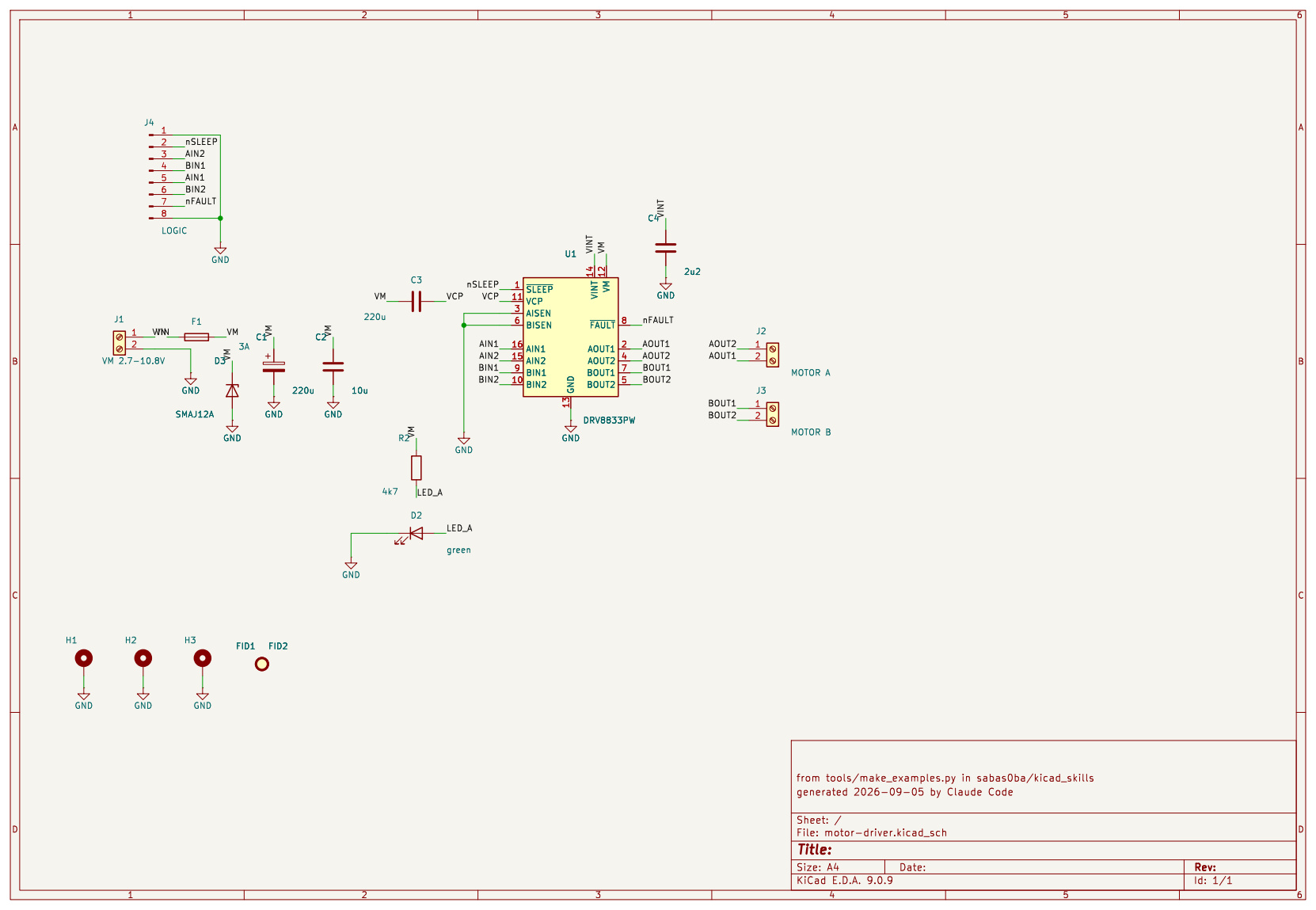
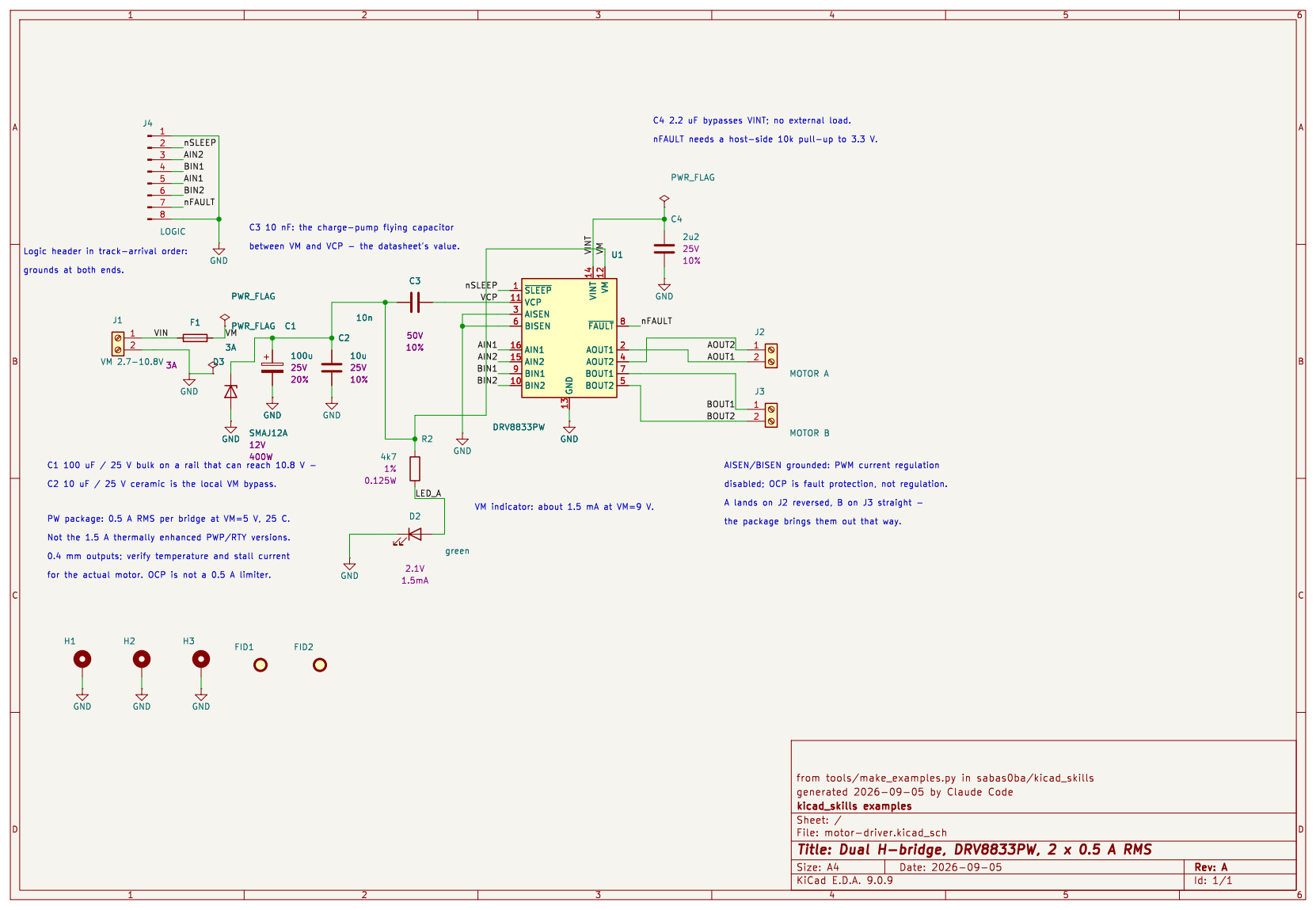
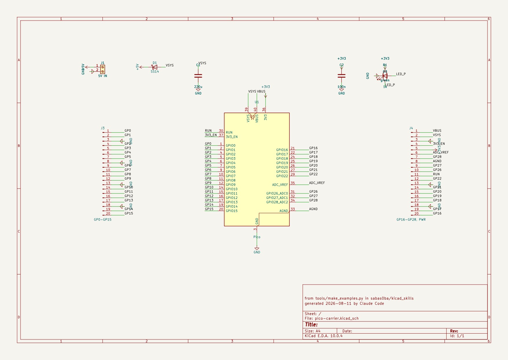
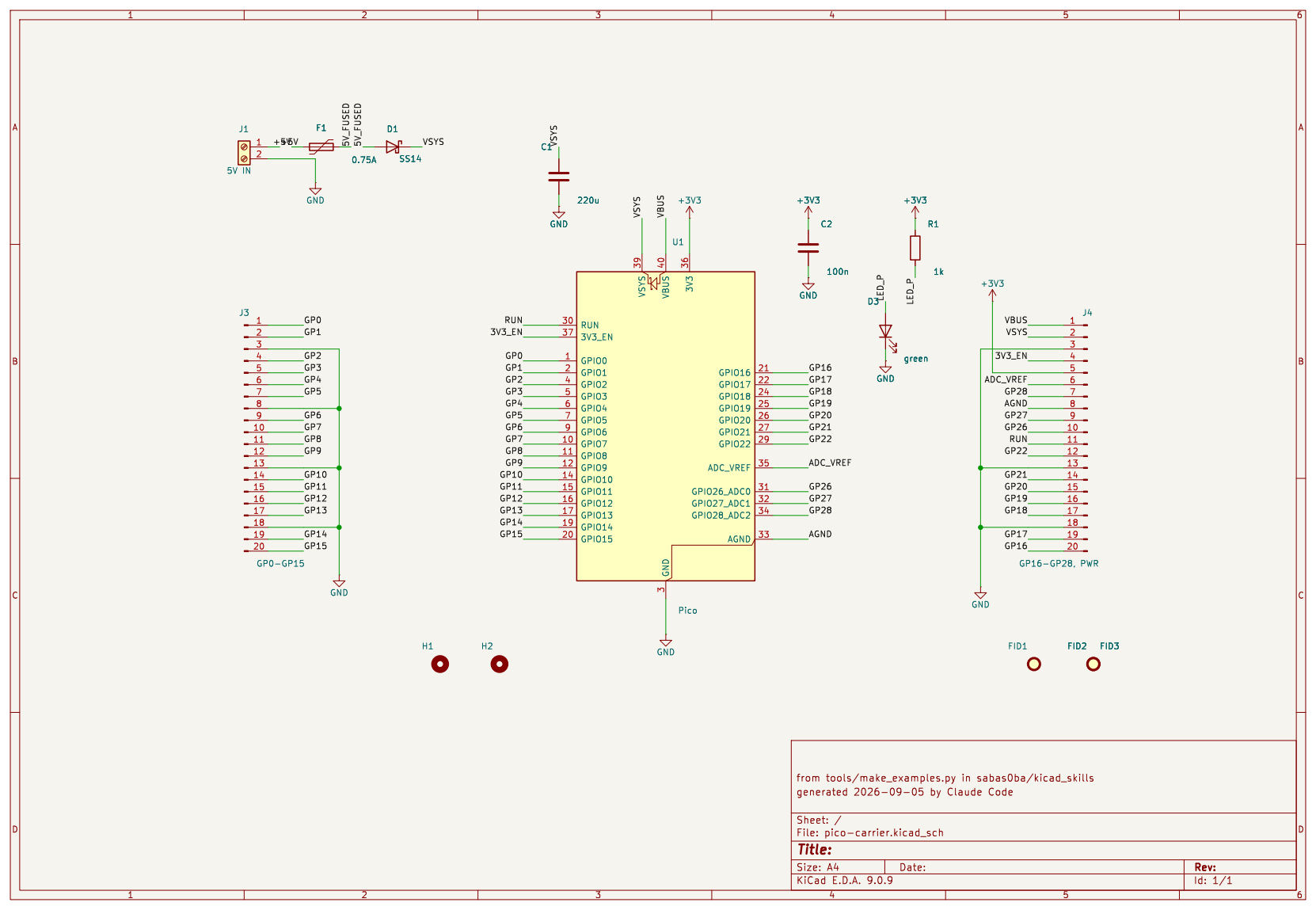
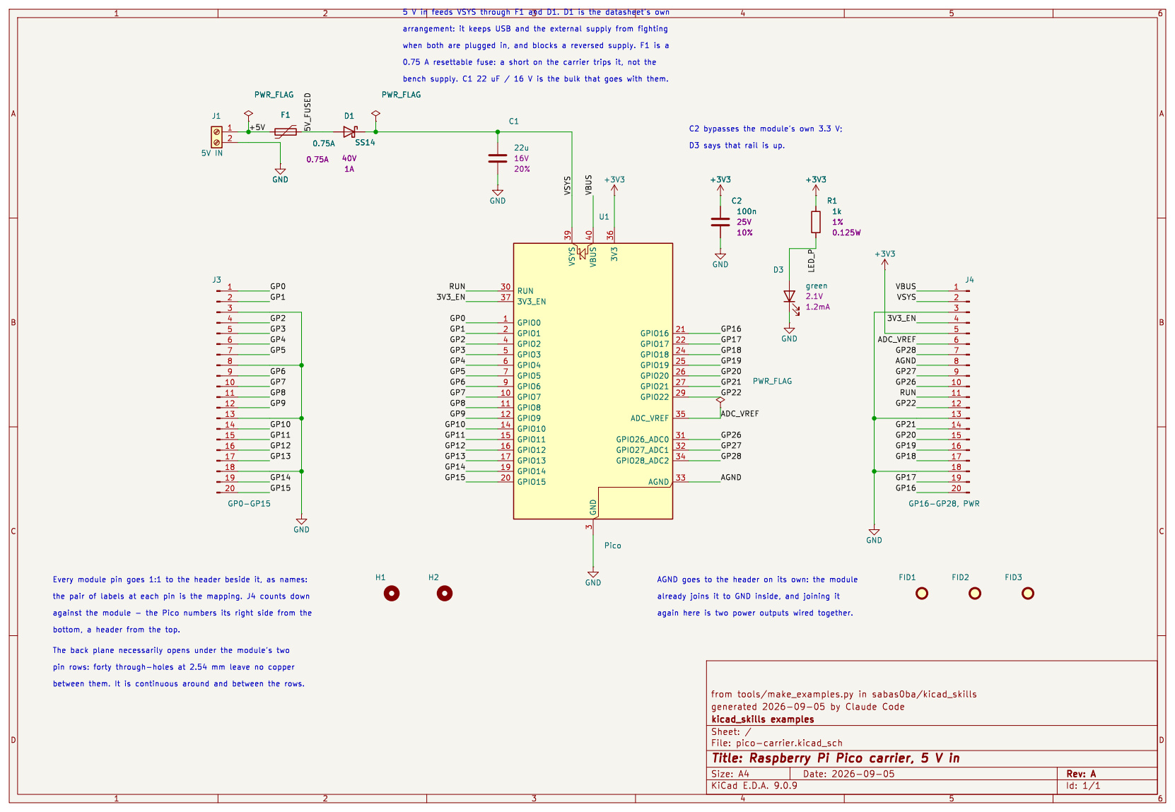
The schematic. Left is the first edition; middle is what the generator leaves today; right is after the loop. The empty title block, the parts stacked on each other at the bottom right, and the absence of any note explaining a single value are all visible before reading one finding:
| first edition | as-generated | reviewed |
|---|---|---|
 |
 |
 |
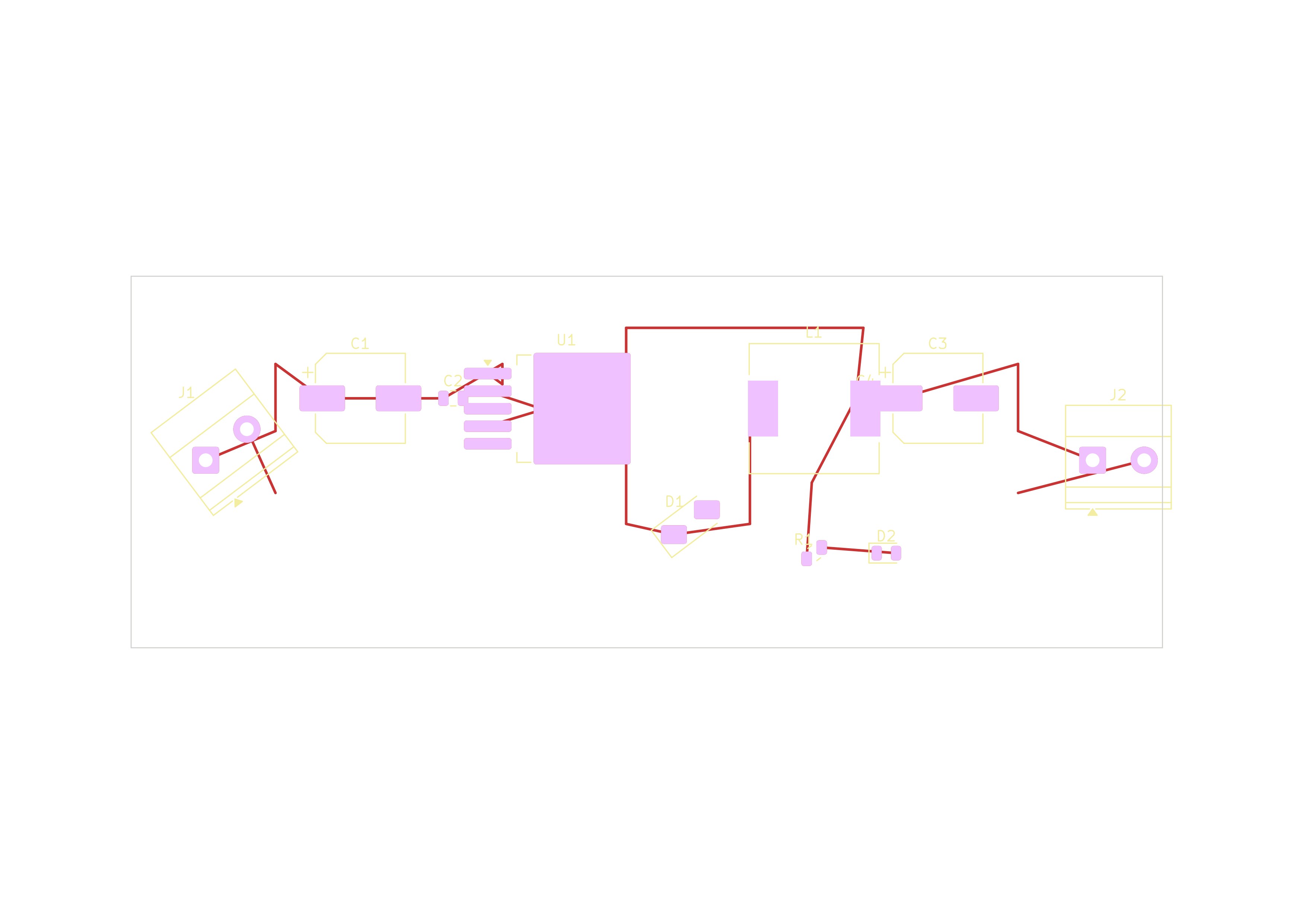
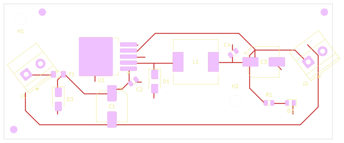
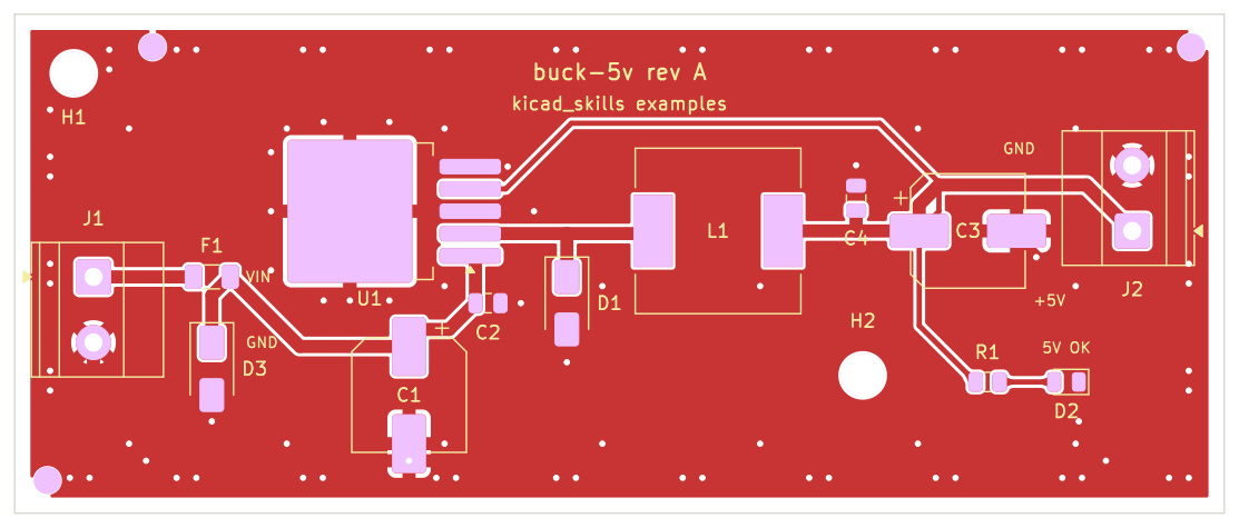
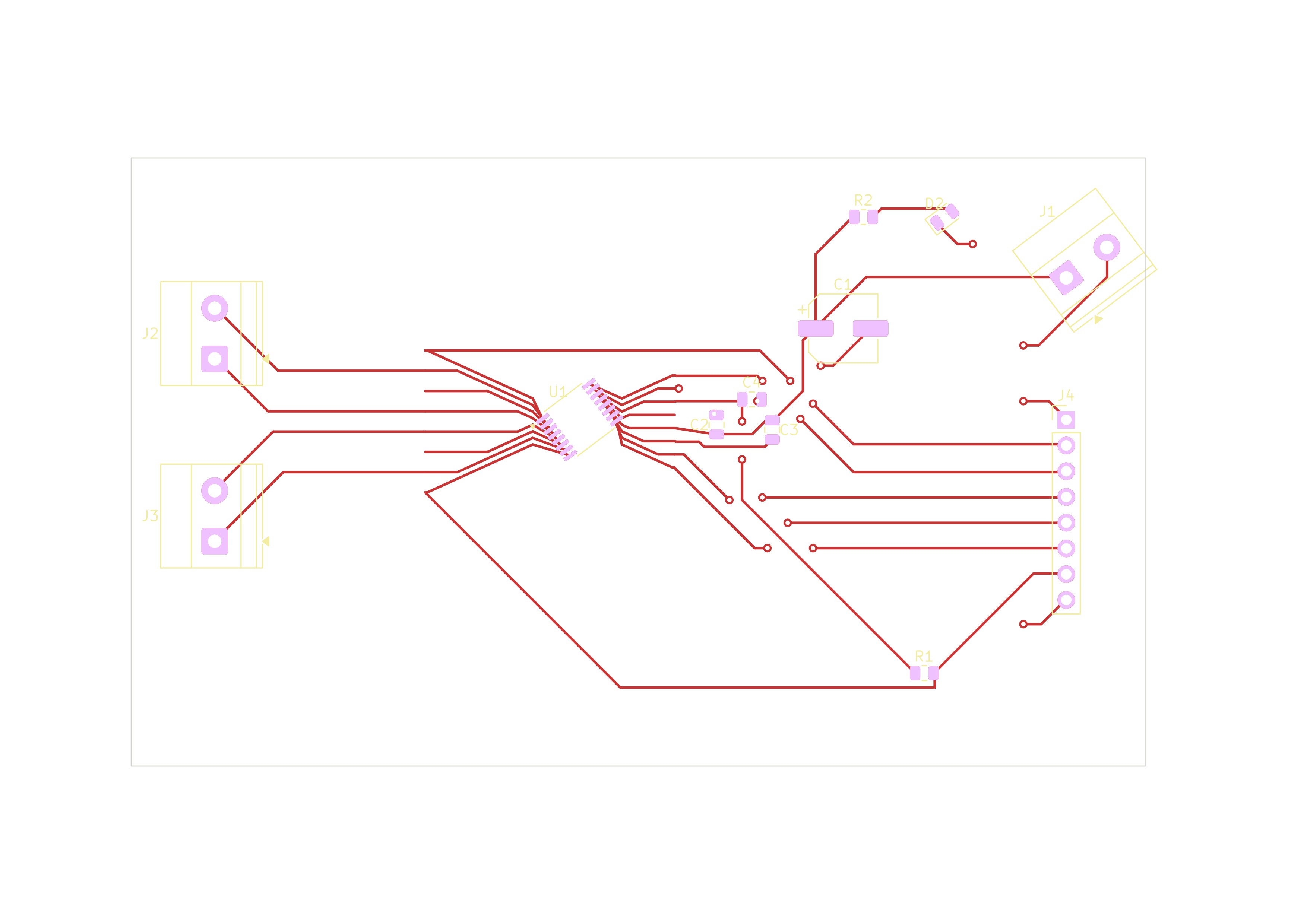
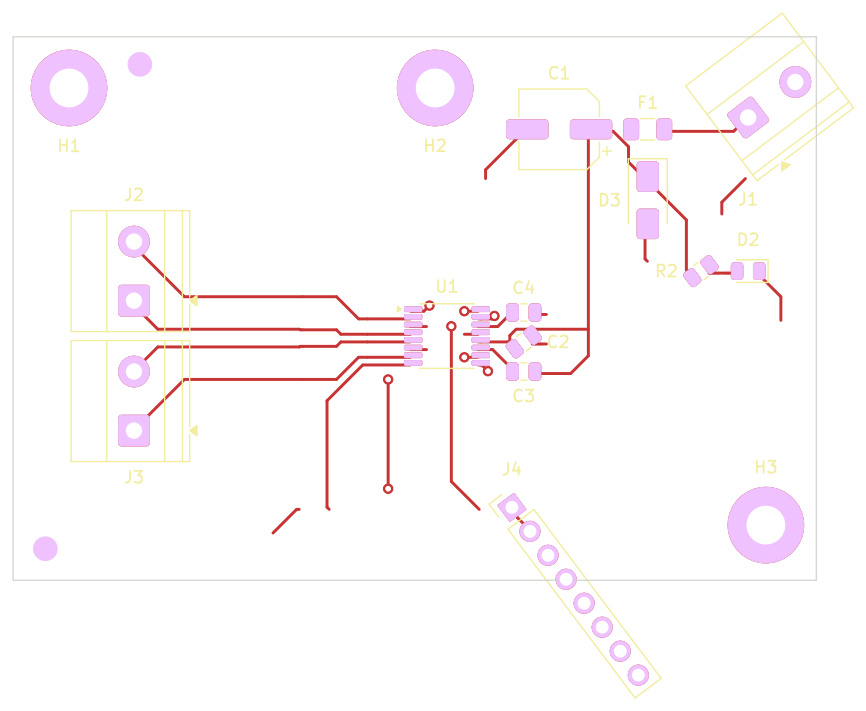
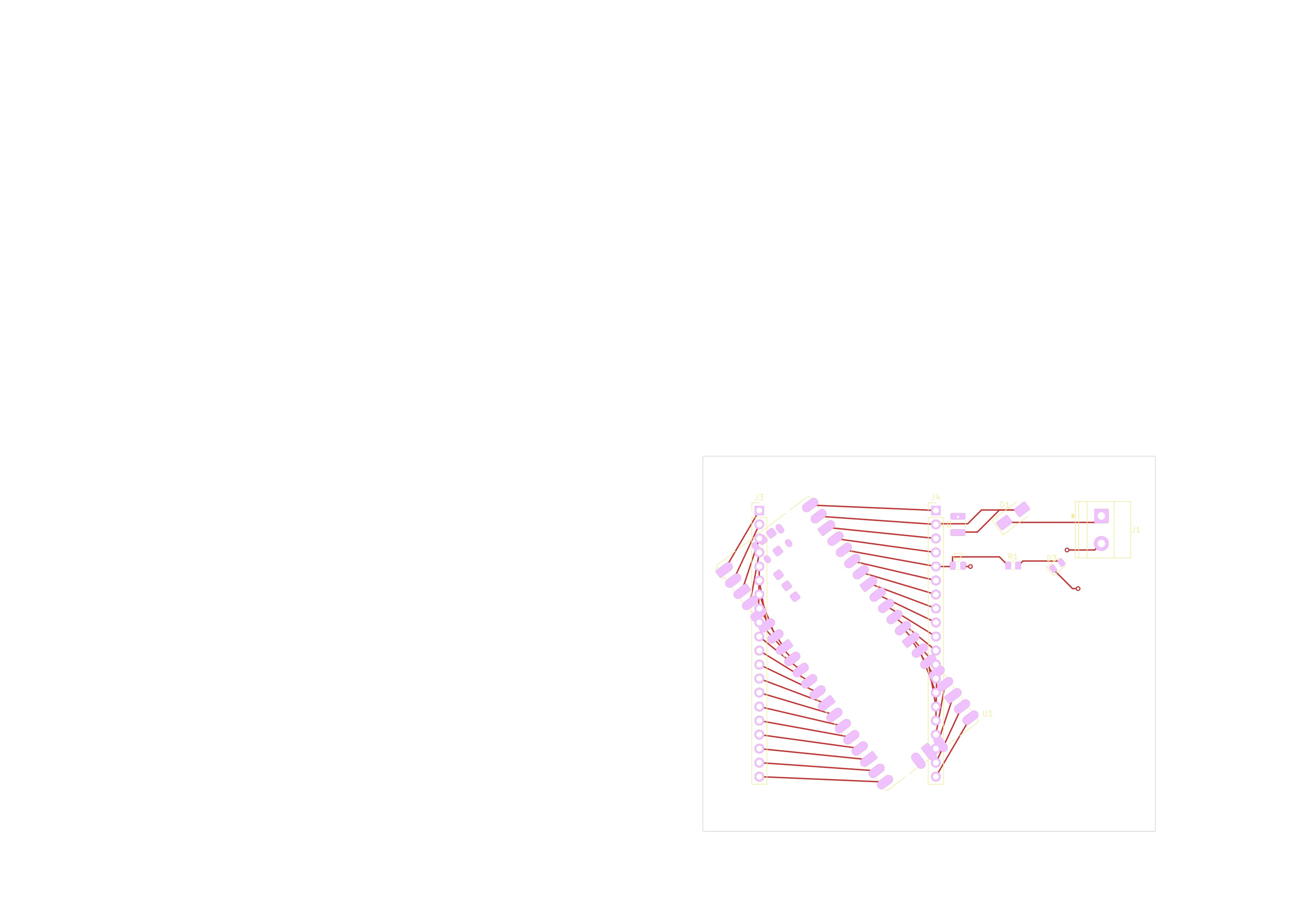
The board, front copper. The same circuit, the same nets. On the left the power rails are routed at signal width, J1 and D1 sit at 37°, and several tracks simply stop in mid-air. On the right the power copper is 1.0 mm, every part is square to the grid, and each ground stub ends in a via:
| first edition | as-generated | reviewed |
|---|---|---|
 |
 |
 |
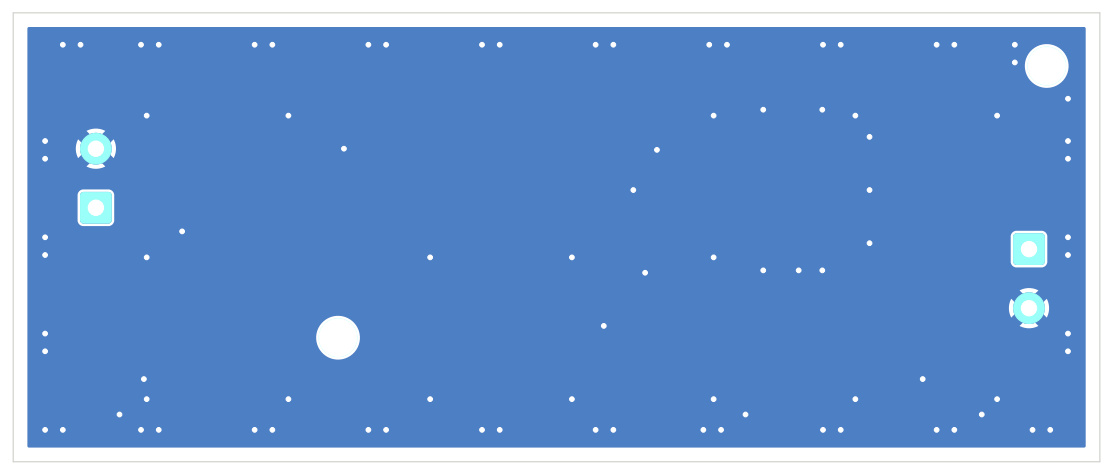
The board, back copper. This is the ground plane, and the reason the floorplan is what it is. Only the two screw terminals are through-hole, and both sit outside the pour, so the bottom layer carries nothing but the plane and the vias dropping into it. Ground now pours on both faces — the front copper joins through-hole only, so no thermal spoke is hostage to a crowded pad — and a ring of stitching vias around the rim ties the two planes together where edge noise wants a short way home. The generated variant has no pour at all:
| first edition | as-generated | reviewed |
|---|---|---|
 |
 |
 |
Both variants also produce a complete fabrication package —
eda pcb fab examples/buck-5v/reviewed -o fab/ writes the gerbers, the Excellon
drill file, the pick-and-place and the BOM.
What separates them, and which check finds it:
in as-generated |
found by |
|---|---|
| symbols and wires off the 1.27 mm grid | readability.off_grid_pin / _wire / _label, and KiCad’s own erc.endpoint_off_grid |
| no PWR_FLAG on the externally supplied rails | erc.power_pin_not_driven |
| two symbols dropped on the same spot | readability.overlapping_symbols |
| no title block, no design notes | readability.title_block, spec.no_design_notes |
| no tolerance / voltage / current rating, no MPN | spec.missing_rating, spec.missing_part_number |
| capacitors chosen without derating the rail | spec.voltage_derating |
| no ESR stated on the output capacitor the regulator’s loop depends on | spec.missing_esr |
| no ground pour | layout.no_ground_plane |
| parts off the placement grid, turned to 37 degrees | layout.off_grid_placement, layout.odd_rotation |
| power routed at signal width | track.thin_power |
| routing left half finished | route.stub, route.acute_angle |
reviewed carries one waiver, in buck-5v/gate.toml:
layout.decoupling_distance on U1.4, because that pin is FB — a sense input, not
a supply — and the rule cannot tell the two apart from the board alone. That is
the mechanism working as intended: the finding is not silenced, it is answered.
What building it changed in the toolkit
Laying out a real board found four things the rules and the parser had wrong:
sexp.dumpswrote every string unquoted, so KiCad refused the generated file.layout.decoupling_viameasured to the pad centre. A bulk electrolytic has a 2.5 mm pad, so the rule asked for a via inside the pad it was meant to sit beside.route.acute_anglecompared against 90° with a 1e-6 epsilon, and a corner drawn at exactly 90° comes out of the arc cosine a ten-thousandth under it.layout.decoupling_viafired on every capacitor sitting in a pour on its own layer, where there is no via to be near — 26 findings across the KiCad demo corpus, 18 of them false.
motor-driver — dual H-bridge, DRV8833PW, 2 × 0.5 A RMS
Two brushed DC motors, screw terminals out, an eight pin logic header, the charge pump and bypass capacitors, and a fuse and a TVS on the motor supply. The PW package is rated at 0.5 A RMS per bridge at VM = 5 V and 25 °C, not the 1.5 A of the thermally enhanced PWP/RTY packages. Confirm temperature and motor stall current for the actual load. TI DRV8833 datasheet.
| verdict | schematic (e/w/i) | board (e/w/i) | |
|---|---|---|---|
reviewed |
PASS, gate exceptions documented | 0 / 0 / 0 | 0 / 0 / 5 |
as-generated |
FAIL, blockers retained | — | — |
| first edition | FAIL, 43 blocking | — | — |
The policy retains two waiver decisions in
motor-driver/gate.toml,
covering the intentional grounded sense pins and the small set of logic nets
drawn as named connections. Grounding AISEN/BISEN disables PWM current
regulation; overcurrent fault shutdown is not a 0.5 A current regulator.
REVIEW.md is the pass that decided them.
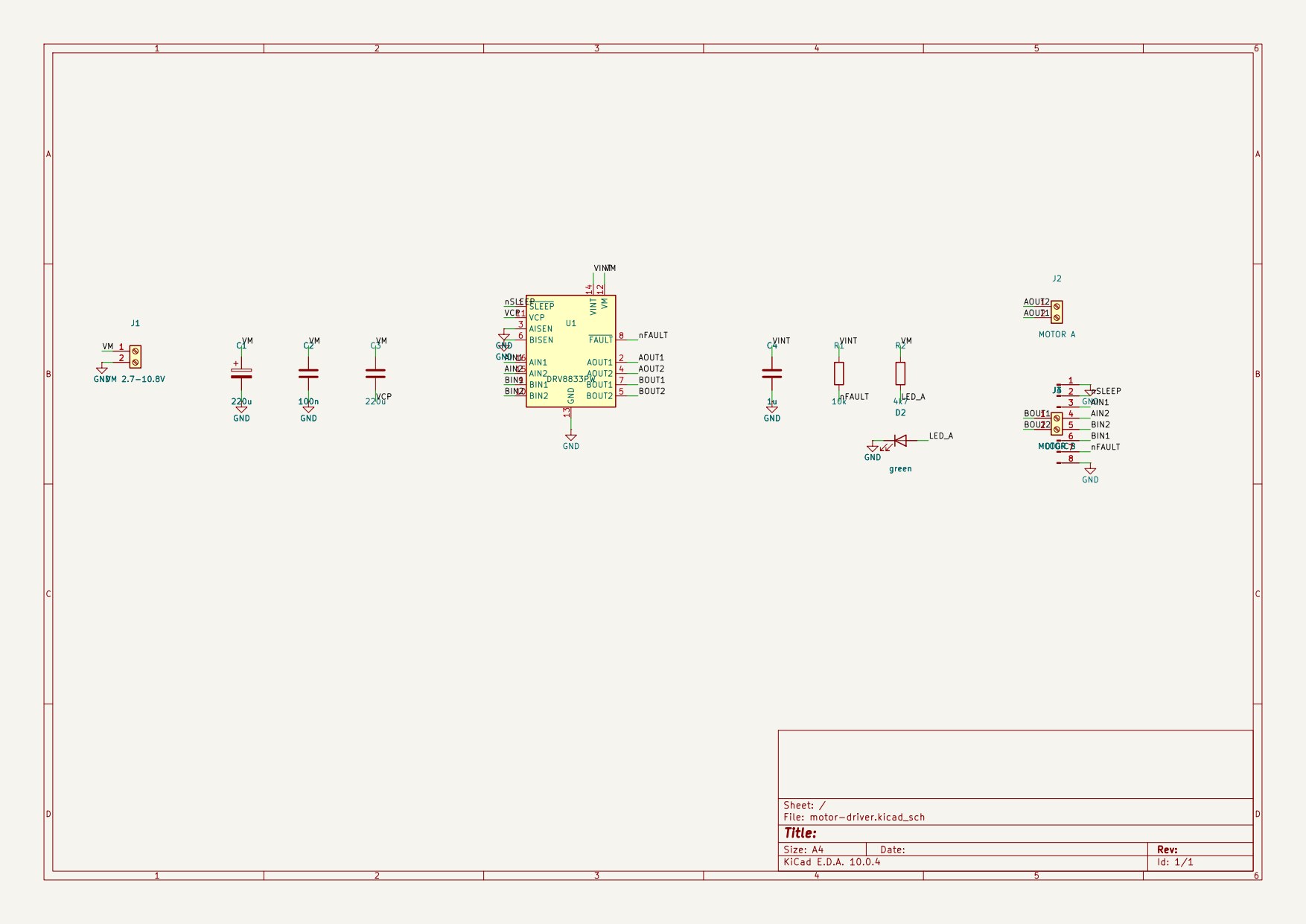
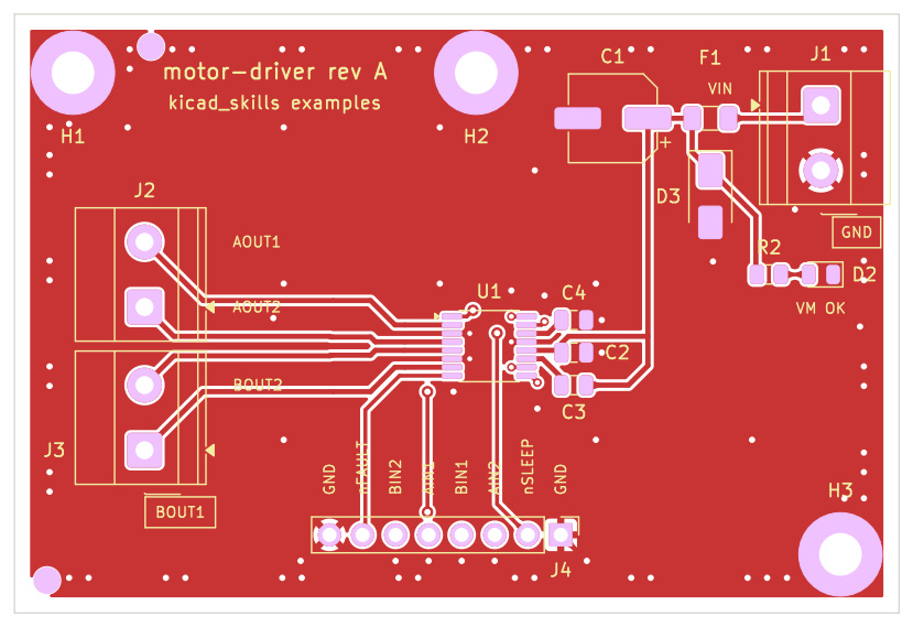
| first edition | as-generated | reviewed |
|---|---|---|
 |
 |
 |
 |
 |
 |
 |
 |
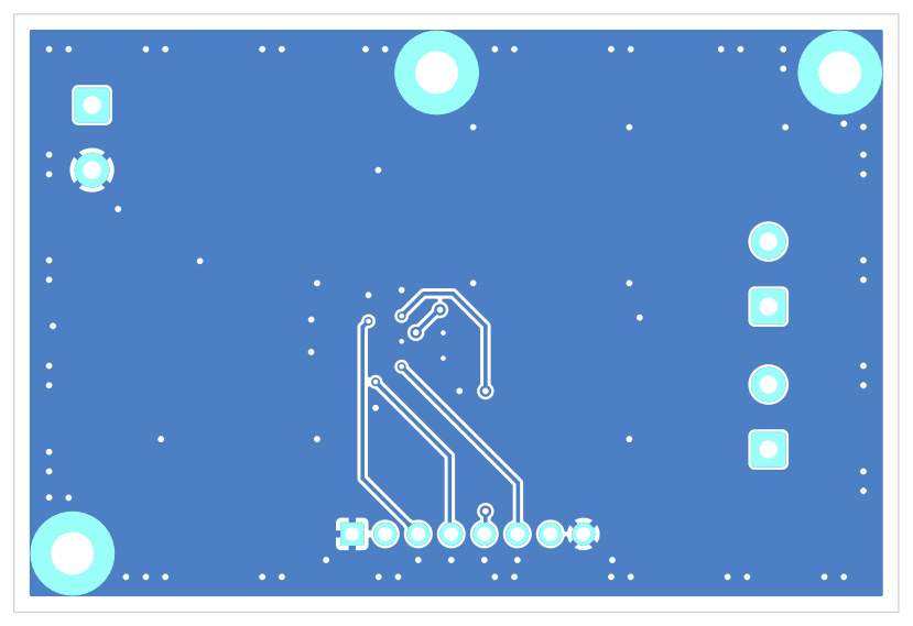 |
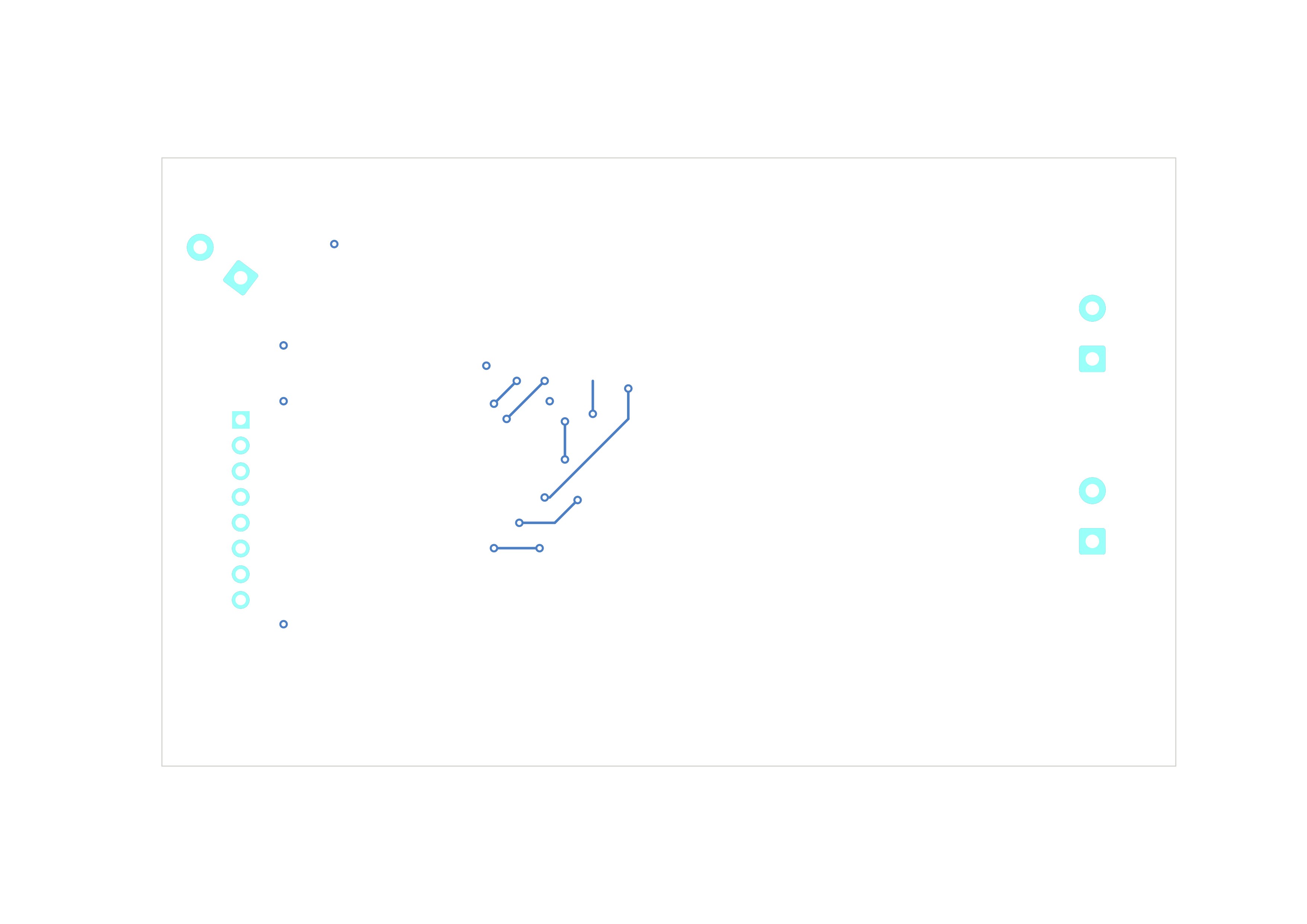
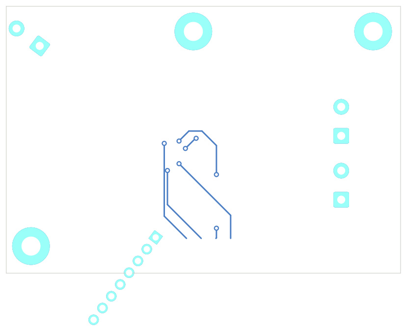
The back layer is the ground pour and the four logic lanes that cross under the bridge outputs, which leaves the front free for the supply row and the local bypass. VM reaches the driver down a stated front-side spine rather than through a plane: the board is two-layer on purpose, and the spine is what that decision looks like in copper.
What this one is honest about
The first rebuild still placed C2/C3/C4 about 12 mm from their IC pins. That was a consequence of the chosen long escape fan, not an unavoidable TSSOP constraint. The follow-up puts all three capacitors beside the supply row, drops the logic locally to B.Cu, and takes the IC grounds straight into the back-layer pour through their own vias. The decoupling-distance waiver is removed; the normal 5 mm limit applies. The generated board measures 2.69 mm from VM to C2, 2.88 mm from VINT to C4, and 3.37 mm from VCP to C3 (pad centres, not complete current-loop lengths).
C2 is now 10 µF on VM, C4 2.2 µF on VINT, and the 10 nF C3 remains between VCP and VM. R1 is removed: VINT is only bypassed, and J4.7 nFAULT requires a host-side 10 kΩ pull-up to 3.3 V. The example-specific CI contract checks these values and exact connections in both schematic and board. It does not verify effective MLCC capacitance under DC bias, thermal performance, motor protection or EMC; those remain application-specific design work.
What building it changed in the toolkit
- The board net names were wrong. KiCad names a net after the sheet path
of the label driving it —
/VM, notVM— and only a power symbol keeps its bare name. That was 35net_conflictfindings on this board and none on buck-5v, because buck-5v’s rails all came from power symbols. - Rotated footprints did not carry their pads’ orientation, which is one
lib_footprint_mismatcheach. Fixing it took buck-5v from three DRC warnings to none. - Footprints had none of the symbol’s fields on them. KiCad’s own “update PCB from schematic” copies them across and then its parity check compares the two; without them that is one finding per field per part.
pico-carrier — Raspberry Pi Pico, every pin broken out
A carrier board: the module, two twenty-pin headers beside it, and a 5 V input that reaches VSYS through a resettable fuse and then the Schottky the Pico datasheet asks for.
| verdict | schematic (e/w/i) | board (e/w/i) | |
|---|---|---|---|
reviewed |
PASS, 9 findings waived | 0 / 0 / 0 | 0 / 0 / 4 |
as-generated |
FAIL, blockers retained | — | — |
| first edition | FAIL, 50 blocking | — | — |
Under KiCad’s own checks reviewed has no errors and no unconnected items, on
9.0.9 and 10.0.4 — one lib_footprint_mismatch on the module and two silkscreen
warnings are all that is left. The gate findings are answered in
pico-carrier/gate.toml;
the schematic-side decoupling rule now reads pin electrical types, so VBUS —
a rail the module drives — is no longer asked for a capacitor at all.
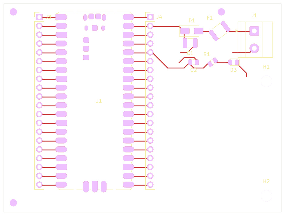
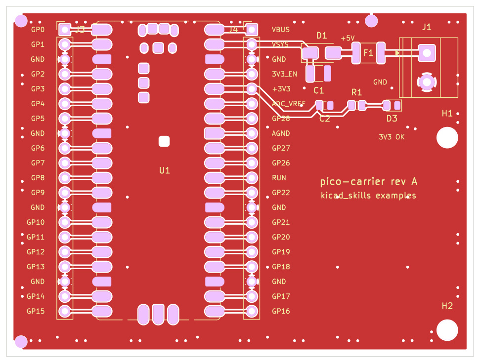
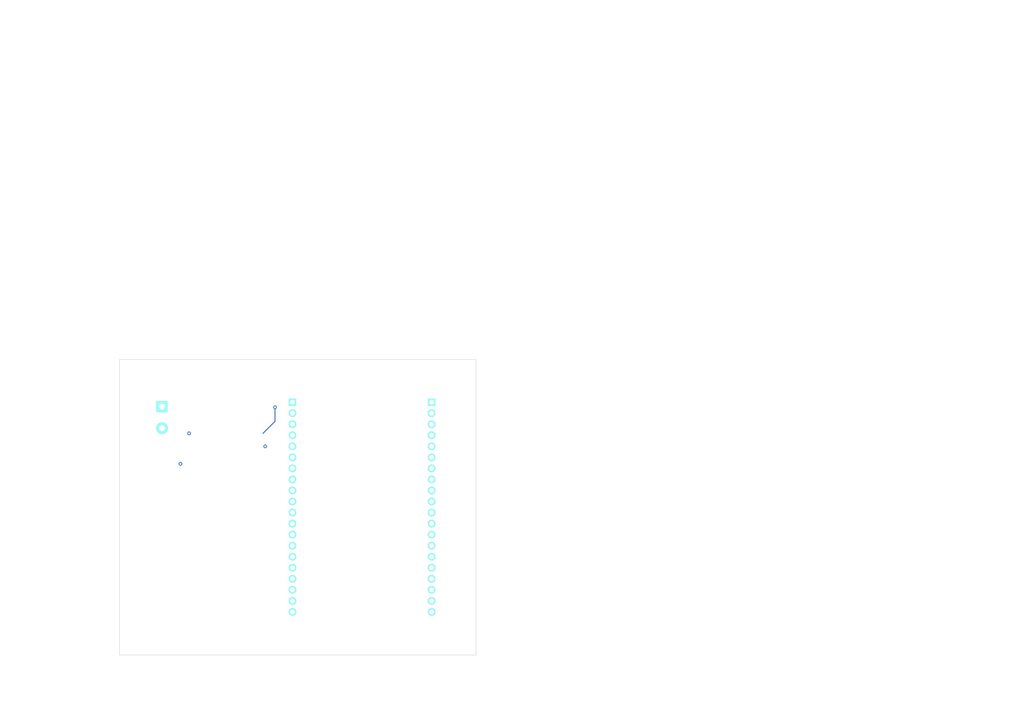
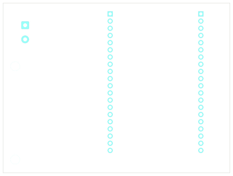
| first edition | as-generated | reviewed |
|---|---|---|
 |
 |
 |
 |
 |
 |
 |
 |
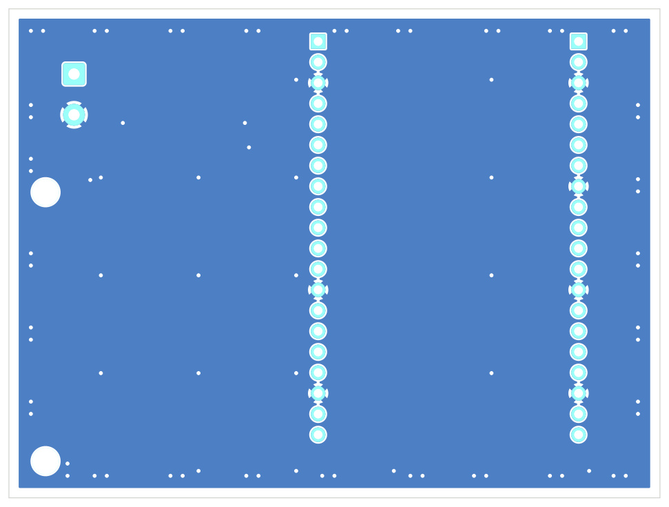 |
What this one is honest about
Most of a carrier is one job done forty times, and the findings are about the few places where it is not:
analog.missing_decouplingandlayout.no_decouplingon VBUS and ADC_VREF — both are rails the module drives and this board merely exposes. The rules cannot tell a supply this board makes from one it is handed, so they ask for a capacitor on a net whose source is somewhere else entirely.layout.decoupling_distance— 9 to 17 mm, and there is nowhere nearer: the header sits between the module pin and any part, by design, and the strip immediately outboard of the header carries the net name of every one of its twenty pins. A capacitor in that strip would be printed over, which is a pad that will not wet. The capacitors sit as close as the legend allows.layout.off_grid_placement— the module’s pads are on a 2.54 mm pitch, so its origin cannot also sit on 0.5 mm, and the headers have to line up with the pads rather than with the grid. Two footprints, both correct.
What building it changed in the toolkit
- The pinout is read out of the symbol, not typed. Forty pins typed a second time is forty chances to swap two of them, and nothing downstream would notice — the board would simply be a different, self-consistent board.
- Stacked pins are drawn once. The Pico symbol brings its seven grounds out at one point; seven wires and seven ground symbols on that point read as one and review as seven.
- The reference and value now go above and below the symbol, measured from its pins. A fixed offset is right for a two-pin part and lands in the middle of the pin labels of a forty-pin one.
- A power symbol turns to face the way its pin leaves. KiCad draws them pointing down and puts the rail name underneath, which on a twenty-pin header is the next pin’s label.
- Footprint uuids are remapped as a set, references included. KiCad’s
(group ...)lists its members by uuid, and the Pico footprint has six of them; replacing pad uuids one at a time leaves the groups naming things that are no longer there.
opamp-filter — 1 kHz Sallen-Key low pass, single 5 V
Two MCP6001 singles: one is the filter, the other buffers the half-rail the filter is referenced to. The supply comes in through a fuse and a TVS, and the output leaves through a 100 ohm isolation resistor before its coupling capacitor.
| verdict | schematic (e/w/i) | board (e/w/i) | |
|---|---|---|---|
reviewed |
PASS, 5 findings waived | 0 / 0 / 0 | 0 / 0 / 4 |
as-generated |
FAIL, blockers retained | — | — |
| first edition | FAIL, 33 blocking | — | — |
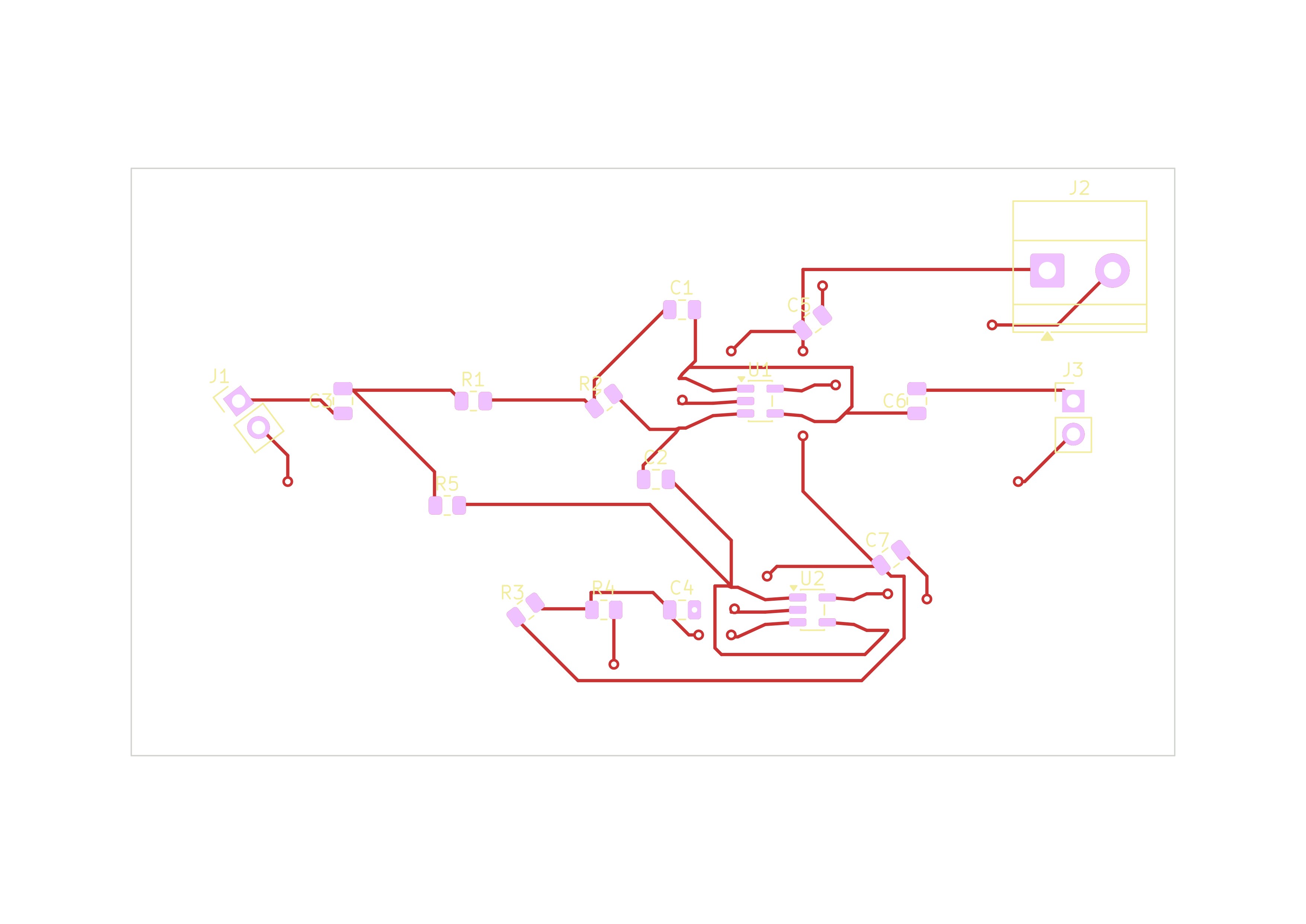
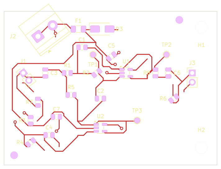
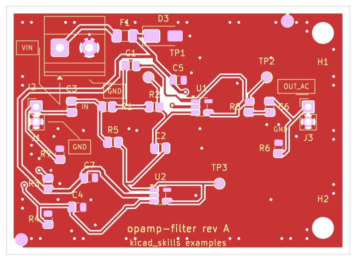
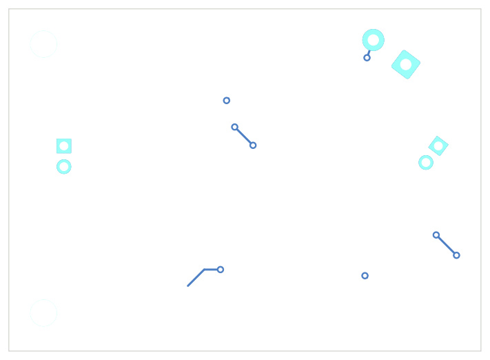
reviewed passes KiCad’s own DRC with two silkscreen warnings — no
errors, no unconnected items, no parity findings. It also passes its own
gate now. The route.wander finding it used to carry was /OUT’s feedback
wrap: thirteen millimetres from one side of the op-amp to the other, routed
last, taking fifty-six millimetres round the board because everything nearer
was already spoken for. Routing it first costs nothing and removes it.
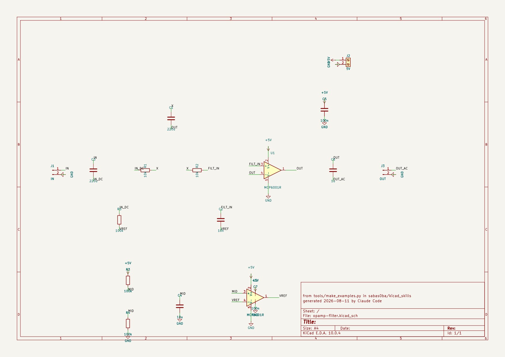
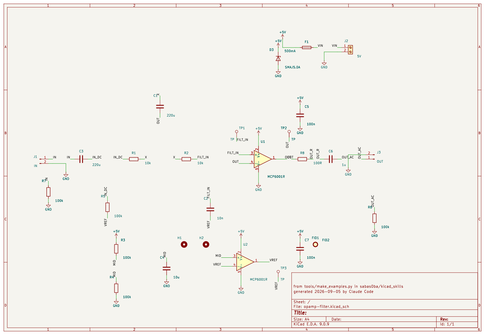
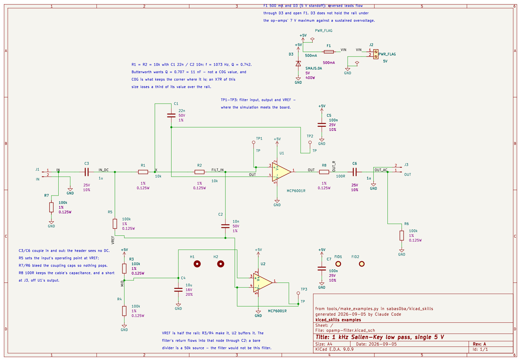
| first edition | as-generated | reviewed |
|---|---|---|
 |
 |
 |
 |
 |
 |
 |
 |
 |
What this one is honest about
layout.decoupling_distanceon VREF (U2.1 and U2.4) — VREF is an op-amp output, the half-rail the signal sits on. It is not a supply and there is nothing to decouple it to; C2 is a filter capacitor that happens to land on that net. This is the same blind spot as VBUS on the Pico carrier, from the other direction.layout.decoupling_distanceon U1.2 and U2.2 — 7.3 mm, and a SOT-23-5 is the reason: three pads at 0.95 mm with the supply in the middle, so the row has to be walked out before anything can be placed against it. Exactly the motor driver’s problem two package sizes down, which is what makes it worth reporting as a pattern rather than as four separate boards’ bad luck.analog.missing_decouplingon VREF — same net, same reason.
The most recognisable generated-schematic trait — every connection a label,
not a wire — is now both measured and fixed. readability.label_only
counts it (this sheet was 96% labels; KiCad’s own demo sheets pass), and the
generator routes the sheet: every one of this design’s eight signal nets is a
drawn wire tree, from the jack through the filter to the jack, with junction
dots where the trees branch, and the rule no longer fires at all. One label
per net survives, because the label is what names the net. This round also
added R6 and R7 — the coupling caps’ far sides previously floated, which the
new analog.no_dc_path rule now catches from the netlist alone.
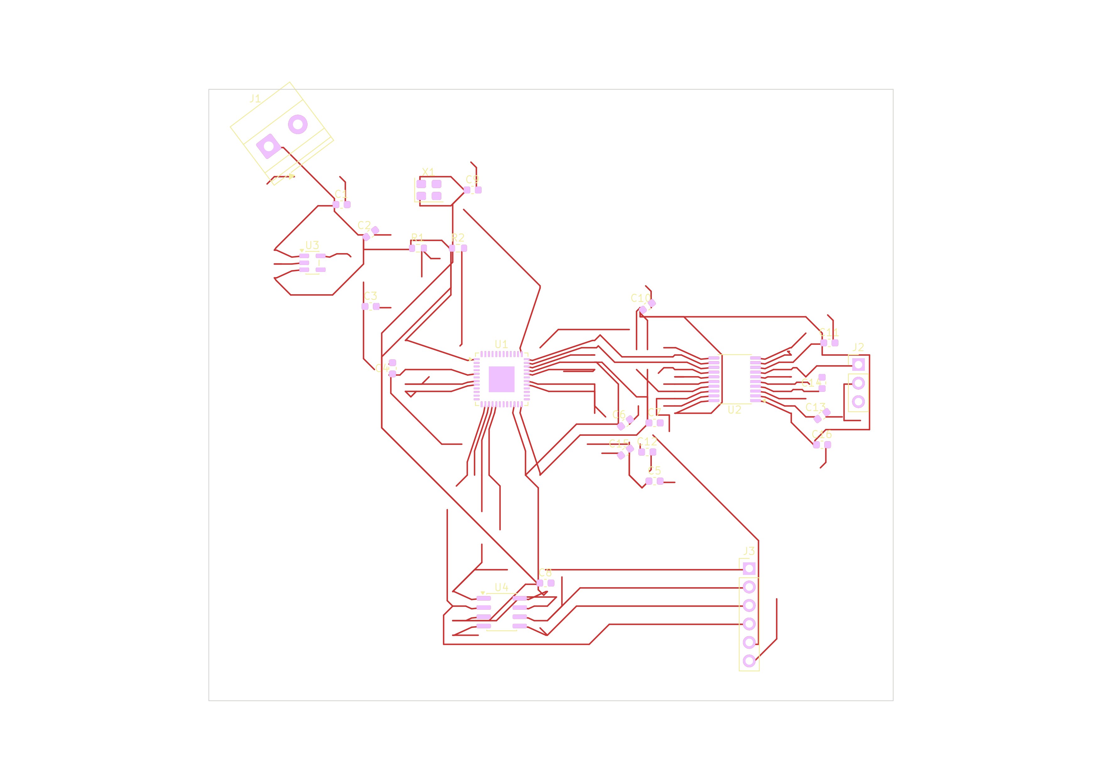
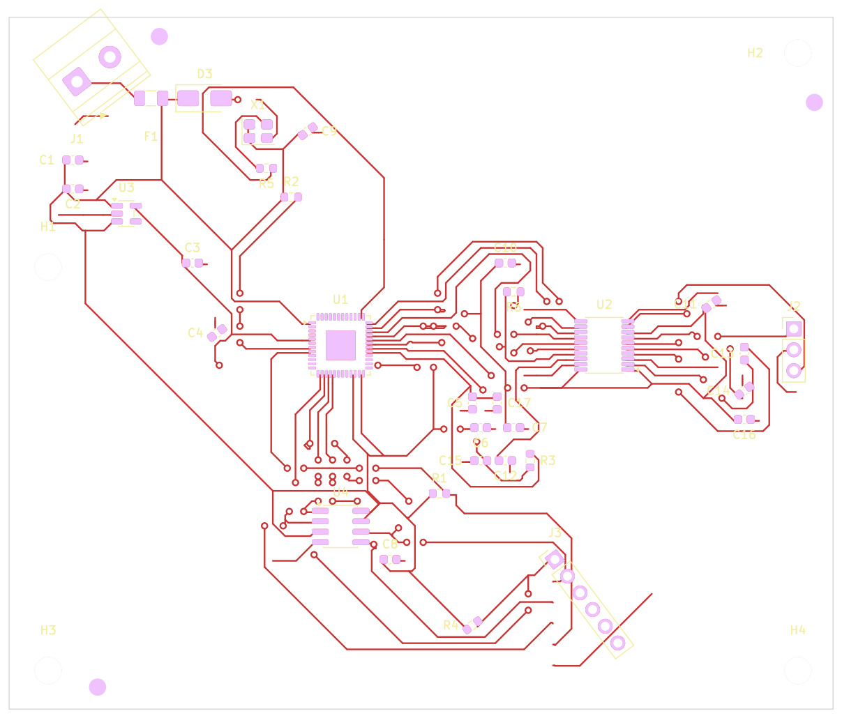
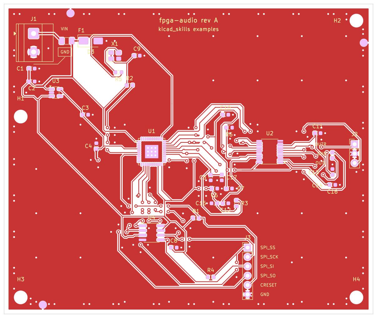
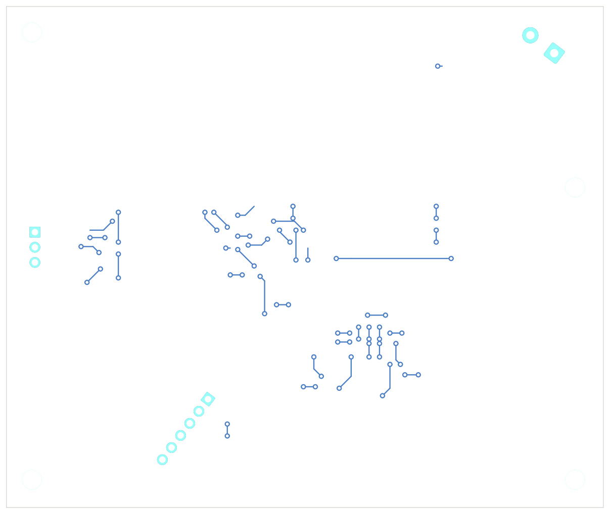
fpga-audio — iCE40UP5K to PCM5102A, I2S out
An FPGA, an I2S DAC, the SPI flash the FPGA boots from, a 12 MHz oscillator and a 1.2 V regulator for the core — on two layers. The 3.3 V input is fused and clamped, the clock leaves the oscillator through a series resistor, and the DAC’s mute is held by a pull-down until the configured FPGA releases it.
| verdict | schematic (e/w/i) | board (e/w/i) | |
|---|---|---|---|
reviewed |
PASS, gate exceptions documented | 0 / 0 / 0 | 0 / 0 / 5 |
as-generated |
FAIL, blockers retained | — | — |
| first edition | FAIL, 34 blocking | — | — |
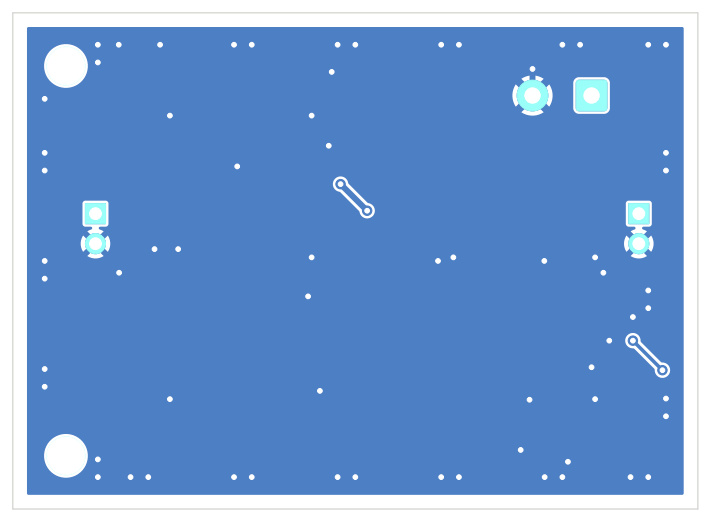
Under KiCad’s own checks reviewed is clean: no DRC errors, nothing
unconnected, no schematic-parity findings. This is the board that pays for the
two-layer rule in area: a 48-pin QFN, a codec, a boot flash and an oscillator
escaped on two layers need 100 x 84 mm, where four layers fitted the same
circuit into 76 x 58 mm. Area is the cheaper currency. The FPGA, codec, flash
and regulator still form one signal-flow block; the line-out and configuration
headers sit on the edges they serve, and the +3V3 distribution is outer-layer
copper rather than a plane. Four ordered I2S runs cross on B.Cu, and the short
+1V2 spine runs there under its own FPGA block.
The earlier engineering pass also fixed four electrical faults that the new floorplan retains: the PCM5102A charge pump is CAPP–CAPM with a VNEG reservoir, VCCPLL is RC-filtered from the core rail, the boot flash has a chip-select pull-up, and the LDO reservoir is 2.2 uF.
| first edition | as-generated | reviewed |
|---|---|---|
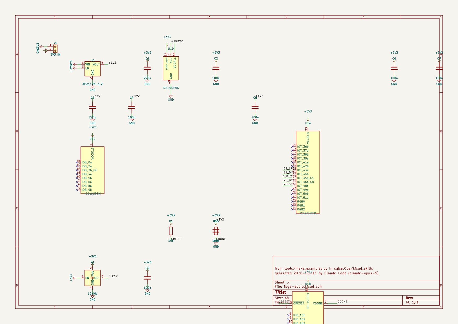 |
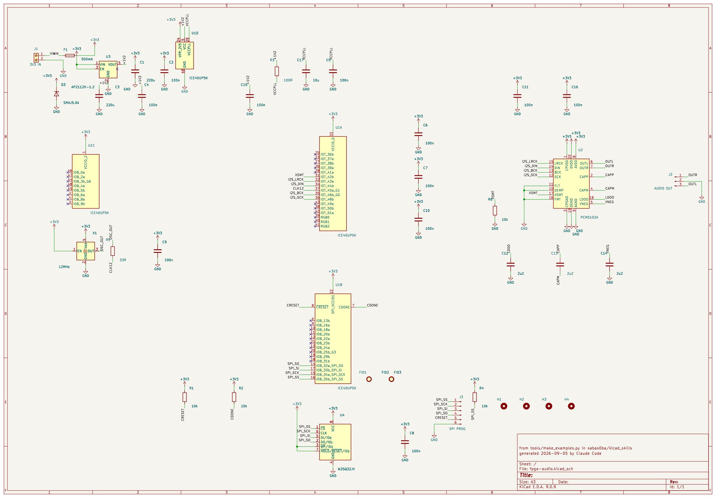 |
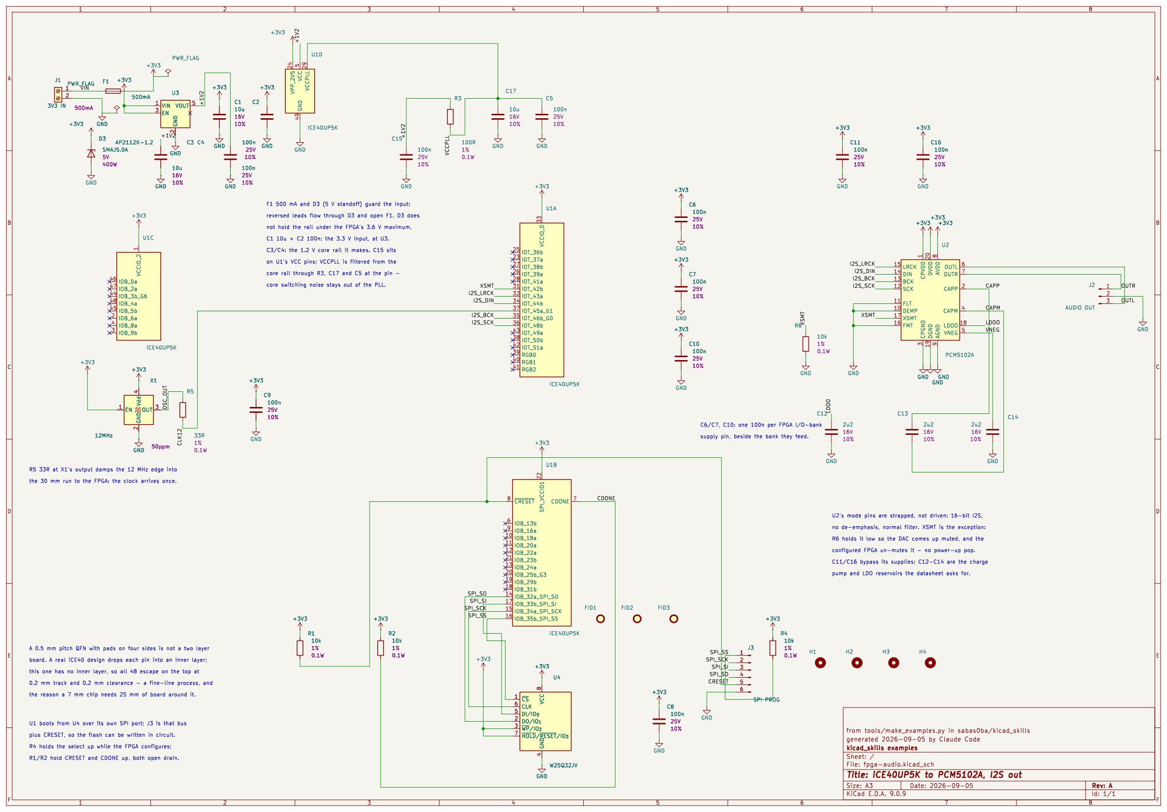 |
 |
 |
 |
 |
 |
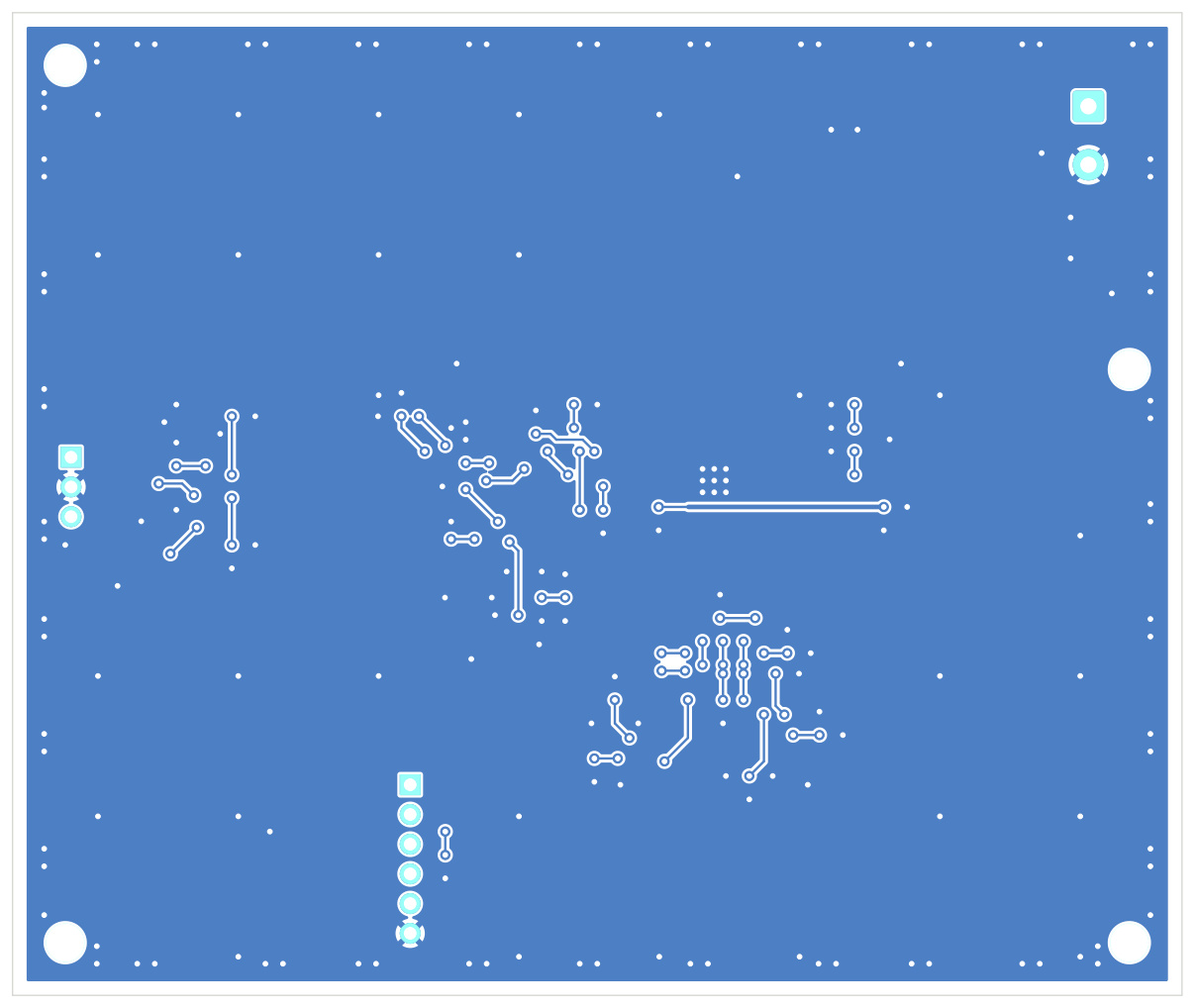 |
These are actual KiCad copper renders. The image utility only removes the empty page margin and converts the format; it does not redraw or rescale copper.
What this one is honest about
Two layers are this example’s design choice, and the area is what it costs. A four-layer stack fits the same circuit into 76 x 58 mm and gives the return path an uncut plane; this board buys neither, and pays in plane cuts, routing tours and 100 x 84 mm of laminate. The trade is stated rather than engineered away, and its long fan and capacitor placement still have room for improvement.
The findings that follow from it, at the scale a 48-pin part gives them:
layout.decoupling_distance× 16 — retained as an explicit limitation of this demonstration floorplan, not an inevitable package constraint. The local ground-via placement is improved, but a short ground stub is not the whole bypass loop. Closer capacitor placement and power-integrity assessment remain open before production reuse.track.thin_powerat 0.2 mm — the escape and +1V2 spine remain narrow. Actual rail currents depend on the FPGA bitstream and IO activity; no firmware-specific power budget has been verified here.erc.pin_to_pinon flash WP/HOLD — the symbol calls these bidirectional quad-SPI pins. This single-bit design straps them high as the datasheet asks; the policy file records why that is intentional.
What building it changed in the toolkit
Five things, each of which had been quietly producing a board that was not the board the schematic described:
- Two nets touching on the sheet is not something an endpoint check can see.
A wire that ends on another wire joins them, and where every pin drags a
stub behind it that is the common case.
schematic_shortslooks for it now and found three here — one had merged the 1.2 V and 3.3 V rails, and the only visible sign was KiCad’s parity check disagreeing about a net name. - A symbol drawn in four units has to be placed four times. All 48 pins
under
(unit 1)leaves three quarters of them in units that were never placed: 25 parity findings, and a sheet nobody can read. - A pin the design does not use still has a net, and a board that leaves the pad bare disagrees with the netlist about every one of them.
- A QFN counts anticlockwise, so its east and north rows run bottom-to-top and right-to-left; handing them to the fan-out in number order made every escape on those sides cross every other one.
- Two rectangles that meet at a corner are further apart than growing both and asking whether they intersect makes them look — which is every pair of pads on the corner of a QFN.
What the five of them say together
Three findings appear on every board that has a fine-pitch part, and they all trace to the same fact — the escape from the package eats the distance budget before any component can be placed:
| motor-driver | opamp-filter | fpga-audio | |
|---|---|---|---|
| package | TSSOP-16, 0.65 mm | SOT-23-5, 0.95 mm | QFN-48, 0.5 mm |
layout.decoupling_distance |
3 | 4 | 16 |
track.thin_power |
0.3 mm | 0.2 mm | 0.2 mm |
The two blind spots that showed up from opposite directions — decoupling asked
of VBUS, which the module drives, and of VREF, which an op-amp output
makes — are closed on the schematic side: analog.missing_decoupling now
reads pin electrical types, asks only where a power_in pin is, and never
asks on a net an output pin drives. The board file carries no pin types, so
the board-side rule keeps its blindness and the waivers say so.
And the two things no rule caught at all became rules in the review round:
- Every connection a label, not a wire →
readability.label_only, plus a sheet router in the generator (straight, L-, Z- and detour-shaped wire trees with junction dots; 0 findings on KiCad’s own demo sheets, and now 0 on everyreviewed/sheet — the handful of nets still labelled are the cross-sheet hauls a human would label too). - Autorouted-looking routing →
route.detour(routed length against the minimum spanning tree of the net’s pads; 0 findings on the demo corpus at the shipped 4x),route.wander(one run of copper against the shortest way round the packages between its own two ends — the net can be the right length and still hold one track that goes out and comes back) androute.return_path(signal over cuts in the other layer’s ground fill — the electromagnetic cost of the two-layer choice). - A tidy route hiding a bad floorplan →
layout.connection_span(the minimum footprint-to-footprint tree before routing exists; pads inside one package collapse to one node). It removed 2 long logical hops from buck-5v, 10 from motor-driver and 13 from fpga-audio before the router was allowed to make their copper look deliberate. - Strings printed through each other →
readability.text_over_text(any two printed strings whose extents overlap — a designator, a value, a rating, a design note or a net label — or any of them across a symbol body). The body is the shape KiCad draws, read out of the schematic’s ownlib_symbols: an LED’s two pins span 2.54 mm and its arrows reach 4.6 mm the other way, so a value cleared of the pins still prints through the part. Nothing about it changes the netlist, so only the plot shows it — which is why every one of these was found by re-rendering rather than by running the tool.
REVIEW.md is the full pass: what was found, what each finding became, and the calibration of every new rule against KiCad’s demo corpus.