 kicad_skills — a containerised circuit-design toolkit





eda is a command-line toolkit for circuit design work: reading datasheets,
simulating analog circuits with ngspice, reviewing KiCad schematics and PCB
artwork, and producing the fabrication package.
Everything runs inside a container. KiCad, ngspice and the Python
dependencies are never installed on the host — the only host requirements are
docker and bash. The KiCad release is a build argument, so it can be pinned
per project.
It is an ordinary CLI that prints JSON and exits non-zero on errors, so it works
the same from a terminal, a Makefile, a CI job, or a coding assistant. The
repository also ships usage guides for each area —
plain Markdown, worth reading on their own, and installable into whatever layout
your assistant expects.
./bin/eda.sh doctor                                   # builds the image on first use
./bin/eda.sh gate        hardware/ --policy ai-generated --text   # pass or fail, and why
./bin/eda.sh report      hardware/ -o build/report    # everything, on one page
./bin/eda.sh sch review  hardware/ --text
./bin/eda.sh pcb review  hardware/ --text
./bin/eda.sh sim run     sim/filter.cir -o sim/out
./bin/eda.sh datasheet parse docs/datasheets/lm321.pdf -o /tmp/ds
Install
Into an existing board project, as a submodule
cd ~/projects/my-board
git submodule add https://github.com/sabas0ba/kicad_skills tools/kicad_skills
./tools/kicad_skills/bin/install-skills.sh
That drops a one-line bin/eda.sh shim so the ./bin/eda.sh … commands work
verbatim from your project root and links the usage guides
into the standard layouts discovered by Codex, compatible assistants, and
Claude Code:
my-board/
├── bin/eda.sh                                    shim -> tools/kicad_skills/bin/eda.sh
├── .agents/skills/kicad-pcb-review/SKILL.md ->   ../../../tools/kicad_skills/docs/guides/kicad-pcb-review.md
├── .claude/skills/kicad-pcb-review/SKILL.md ->   ../../../tools/kicad_skills/docs/guides/kicad-pcb-review.md
├── hardware/my-board.kicad_pro
└── tools/kicad_skills/                           the submodule
Commit bin/eda.sh so everyone who clones the project gets it. Upgrading is
git submodule update --remote — the symlinks follow, with no re-install.
The generated skill layouts are outside the submodule, so add .agents/skills/
and .claude/skills/ to the parent project’s .gitignore unless the project
chooses to track those adapters.
| Flag | Effect |
|---|---|
--no-guides |
just the CLI shim, nothing else |
--dest DIR |
another tool’s directory (e.g. --dest .cursor/rules) |
--copy |
vendor the guides instead of symlinking (Windows checkouts) |
--force / --uninstall |
replace what is already there / reverse the install |
The guides themselves need no install — they are Markdown in
tools/kicad_skills/docs/guides/, readable as they are.
Then, from your project root:
./bin/eda.sh doctor                       # builds the image on first use (~5 min)
./bin/eda.sh report hardware/ -o build/report
Or standalone
No install step is needed to try it — clone and run:
git clone https://github.com/sabas0ba/kicad_skills && cd kicad_skills
./bin/eda.sh doctor            # {"kicad_cli": "10.0.4", "ngspice": "...", "ok": true}
./bin/eda.sh report ~/projects/my-board/hardware -o /tmp/report
bin/eda.sh mounts the git repository root that contains the current directory
at /work, runs as your uid/gid (no root-owned files), and gives the container
no network. To work on the toolkit itself, see AGENTS.md.
If you drive this clone with Codex, another Agent Skills-compatible assistant,
or Claude Code, make skills mirrors the guides into the layouts they discover.
Those directories are generated and git-ignored — the guides live in
docs/guides/.
What it does
flowchart LR
    PDF[datasheet PDF] --> DS[eda datasheet]
    DS -->|part values| SIM[eda sim]
    SIM -->|verified circuit| SCH[eda sch review]
    SCH -->|netlist + ERC| PCB[eda pcb review]
    SCH --> GATE[eda gate]
    PCB --> GATE
    GATE -->|pass| FAB[eda pcb fab]
    SCH --> REP[eda report]
    PCB --> REP
    SIM --> REP
    REP --> HTML[report.html + PNG + PDF + GLB]
| Area | What it does | One command | Guide |
|---|---|---|---|
| Datasheets | Text, parameter tables, embedded figures and rendered page images from a PDF | eda datasheet parse lm321.pdf -o out/ |
guide |
| Simulation | ngspice op/dc/ac/tran/noise, THD, Monte Carlo tolerance analysis, temperature sweeps — with measurements and plots | eda sim run filter.cir -o out/ |
guide |
| Schematic review | Components, nets and hierarchy from .kicad_sch; ERC plus decoupling / floating-input / annotation / pull-up checks, drawing readability (grid, junctions, overlap, page) and part specification (ratings, derating, part numbers) |
eda sch review hardware/ --text |
guide |
| Board review | DRC, schematic parity, track widths, drills, exact board-edge clearance, ground pour, silkscreen over pads, placement grid and rotation, track stubs and acute corners, decoupling vias; current capacity, resistance and impedance from the stackup — closed forms, or a 2D field solve with --solve; a steady-state temperature map and heating curve for stated dissipations (pcb thermal); near- and far-end crosstalk of the coupled runs from solved line matrices (pcb crosstalk); layer plots and 3D renders |
eda pcb review hardware/ --text |
guide |
| Design gate | One pass/fail verdict over ERC, DRC and both reviews against a stated policy; readability, layout-practice and part-specification rules; waivers that must carry a reason | eda gate hardware/ --policy ai-generated |
guide |
| Fabrication | Gerbers, Excellon drill, pick-and-place, BOM, STEP/IPC-2581, zipped with a manifest | eda pcb fab hardware/ -o fab/ |
guide |
| The container | Build, pin, verify and troubleshoot the toolchain | eda doctor |
guide |
Examples
Review a board and see why — findings are structured, so they can be
filtered, counted and gated on in CI; --text is the human digest.
$ ./bin/eda.sh pcb review hardware/ --text
## summary: error=1, warning=3, info=4

## findings
  ERROR   board.copper_outside_outline: 46 copper item(s) lie outside the board outline
  WARNING board.edge_clearance: 2 copper item(s) within 0.3 mm of the board outline
  WARNING layout.decoupling_distance [U3.14 / +3V3]: C12 is 8.4 mm away
  INFO    board.size: board outline is 63.5 x 40.6 mm
Exit code is 2 when a review found errors, so eda pcb review hardware/ is
also a CI gate; -o report.json keeps the structured version.
Hold a generated design to a standard — a review lists what is wrong; a gate says whether that is acceptable, against a policy the project committed to.
$ ./bin/eda.sh gate hardware/ --policy ai-generated --text
# gate FAIL: hardware/ against policy 'ai-generated'

## after the policy: error=11, warning=0, info=2
  over the limit: 11 error(s), 0 allowed

## blocking
  ERROR   schematic/readability.off_grid_pin: 12 pin(s) are off the 1.27 mm grid -
          wires that meet them look connected and are not (reported as warning)
  ERROR   schematic/spec.voltage_derating [/:C7]: C7 is rated 6.3 V and sits on a 12 V rail
  ERROR   board/silk.over_pad: 4 silkscreen item(s) print across a pad (reported as warning)

## waived
  drc.lib_footprint_mismatch: our footprints are project-local copies
None of that is something ERC or DRC has an opinion about, which is exactly why
a design can be ERC-clean, DRC-clean and still be one no engineer would sign.
(reported as warning) is the policy at work — and a waiver without a stated
reason is refused, so nothing is passed over quietly.
eda gate --list-rules prints the whole contract: every rule, the exact
condition that makes it fire, the threshold that tunes it and its default, and
the policies under which it blocks. It is assembled from the rule modules, and
tests/test_rule_spec.py reads their source, so a rule the catalogue does not
describe — or an entry no rule produces — fails the build. See the
design gate guide for the evaluation rules
and the exit codes.
Simulate before committing to a part value — the −3 dB corner, the phase margin and the tolerance spread come back as numbers, not a picture to squint at.
$ ./bin/eda.sh sim montecarlo sim/rc.cir -o sim/mc \
    --vary R1=1% --vary C1=10% --metric 'ac.v(out).f_minus_3db_hz' --trials 200
{"metric": "ac.v(out).f_minus_3db_hz", "nominal_metric": 997.7,
 "statistics": {"samples": 200, "mean": 1001.1, "stdev": 35.5,
                "p05": 940.1, "median": 1000.7, "p95": 1064.0, "spread_pct": 20.4},
 "sensitivity": {"explained_pct": 99.7, "parameters": [
     {"parameter": "C1", "contribution_pct": 99.3, "elasticity": -0.99},
     {"parameter": "R1", "contribution_pct":  0.7, "elasticity": -0.96}]},
 "failures": [], "histogram": "sim/mc/histogram.png", "csv": "sim/mc/trials.csv"}
The 10 % capacitor is the entire spread; the 1 % resistor is noise. That is the line item worth changing, and it came out of the trials that were already run.
Read a datasheet without opening a viewer — page images for the curves, tables for the numbers.
$ ./bin/eda.sh datasheet find docs/lm321.pdf "supply current"
[{"page": 3, "line": "Supply Current  IS  VS = 5 V, no load  0.43  0.75  mA"}]
$ ./bin/eda.sh datasheet pages docs/lm321.pdf -o out/ --pages 7 --dpi 200
One command for the whole project — see the worked example below.
./bin/eda.sh report hardware/ -o build/report --glb
open build/report/report.html
What the gate is worth, in pictures
Five complete designs are generated by tools/make_examples.py
and shipped twice: once as the generator first left them, and once after
eda gate had been run and every finding answered. Same circuit, same nets,
same parts — the difference is entirely what the gate had an opinion about.
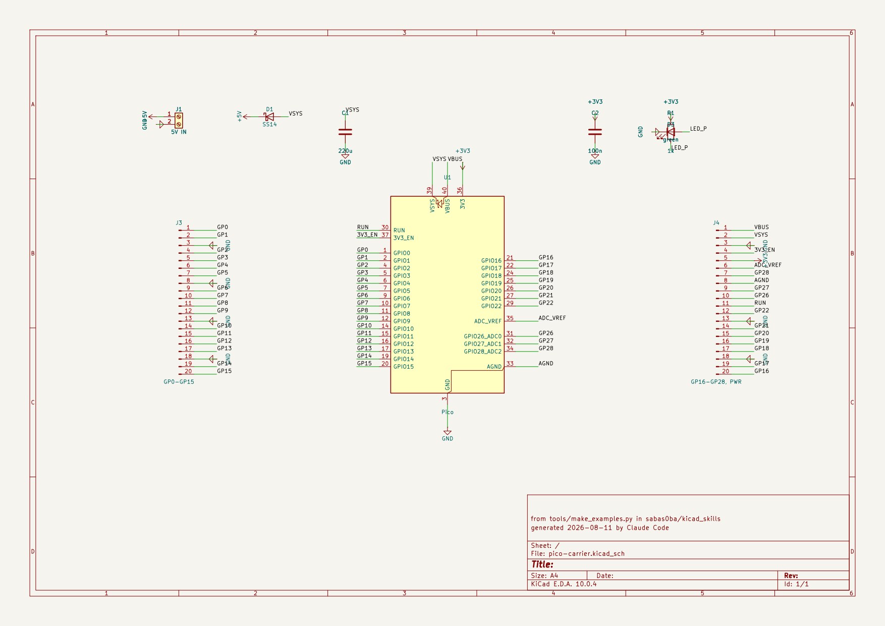
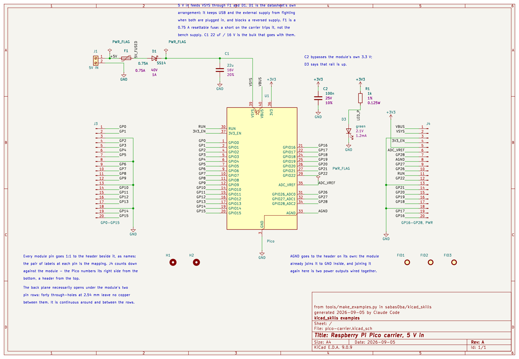
A schematic. The Pico carrier. On the left: an empty title block, not one note, and eighteen power symbols pointing in four different directions. On the right: a title that says what the board is, fifteen notes recording why the values are what they are, and every power symbol upright:
| as generated | after the gate |
|---|---|
 |
 |
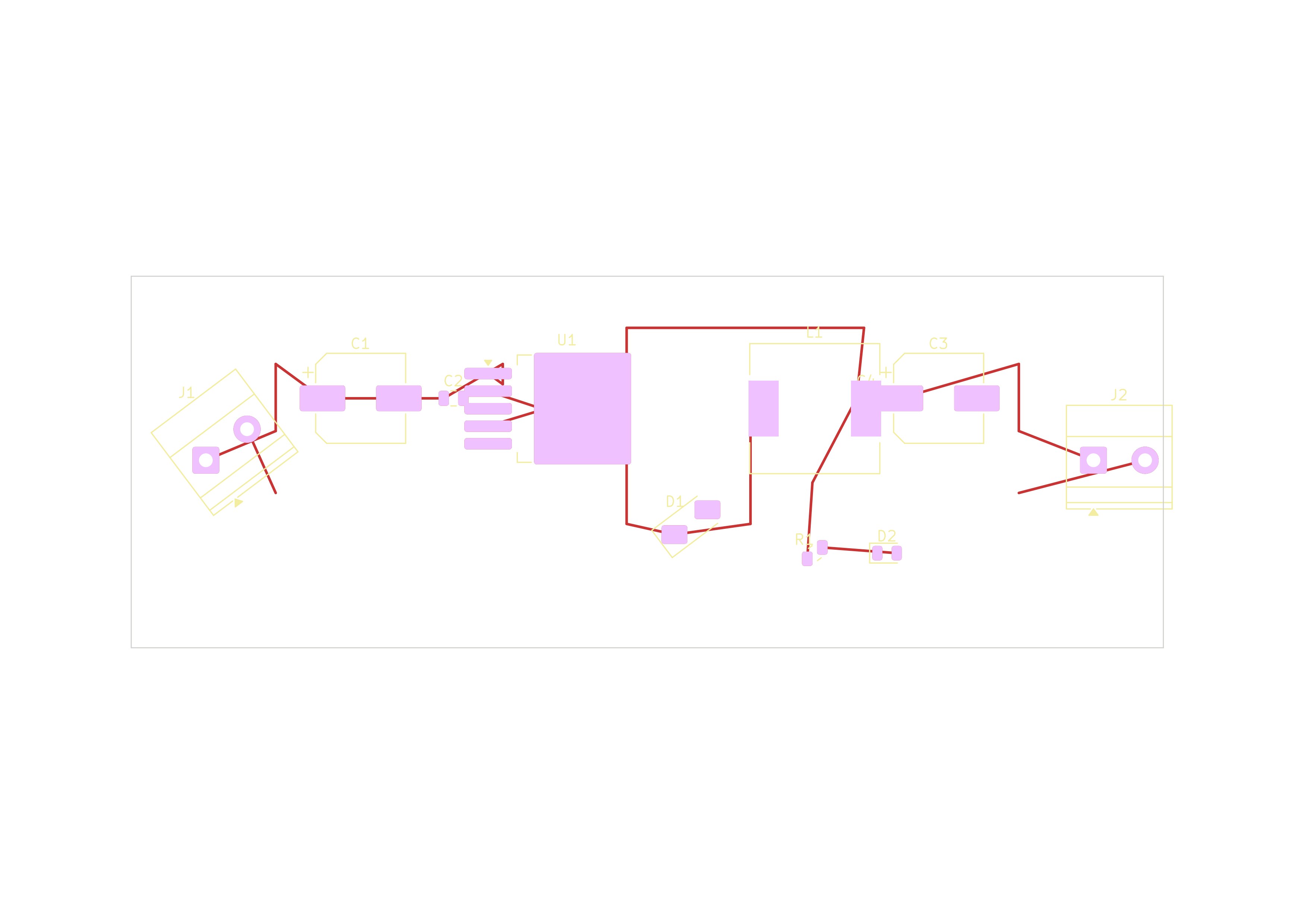
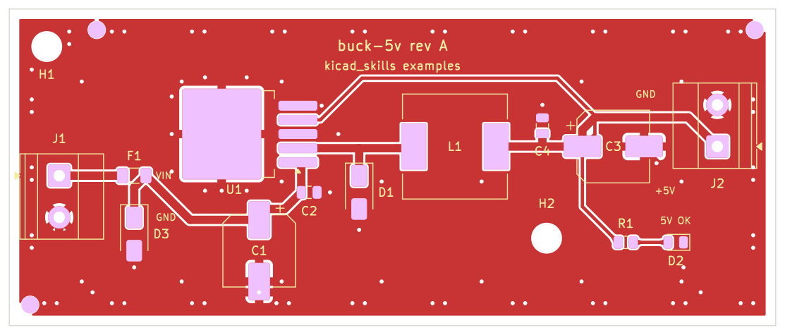
A board. The 12 V → 5 V buck. On the left: no ground pour, not one via, every track 0.25 mm whatever it carries, and nothing on the silkscreen at all. On the right: the plane poured on both faces and stitched with 79 vias, power copper at 1.0 mm and tapered into every land, screw holes that clear an M3 washer, and a regulator tab relieved so a reflow oven can still solder it:
| as generated | after the gate |
|---|---|
 |
 |
And the motor driver, which went from one track width for the whole board to fifteen — motor outputs, logic and the charge pump each sized for what they carry — and gained the plane its H-bridge returns through:
| as generated | after the gate |
|---|---|
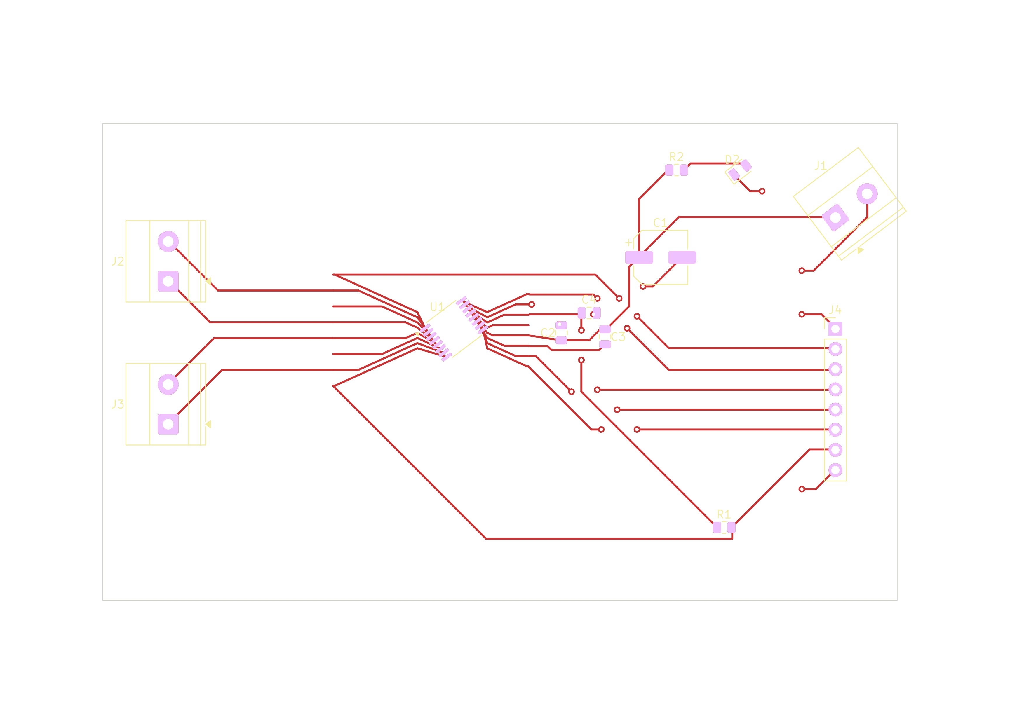 |
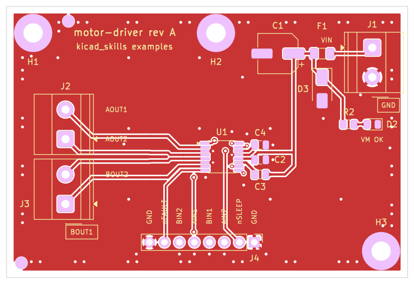 |
The scoreboard, under each project’s own policy:
| design | as generated | after the gate |
|---|---|---|
| buck-5v | FAIL — 45 blocking | PASS |
| motor-driver | FAIL — 43 blocking | PASS |
| pico-carrier | FAIL — 50 blocking | PASS |
| opamp-filter | FAIL — 33 blocking | PASS |
| fpga-audio | FAIL — 34 blocking | PASS |
All five gated boards are clean under KiCad’s own DRC on both versions in the matrix, with nothing unconnected, and every finding that remains is a waiver carrying the sentence that excuses it.
examples/ is the long version: all five designs, both faces of every board, a third column showing what the generator produces today (the reviews went into the generator, not into patches on its output), and REVIEW.md — twenty rounds of a reviewer reading the boards, and what each finding became: a rule, a fix, or a waiver with its argument.
Pinning the KiCad version
KICAD_VERSION=10.0.4 make build     # default, current stable
KICAD_VERSION=9.0.9  make build     # a second image for older projects
KICAD_VERSION=9.0.9 ./bin/eda.sh pcb review board.kicad_pcb
Each version produces its own image tag (eda-toolkit:<version>) so several can
coexist. Tags: https://hub.docker.com/r/kicad/kicad/tags. KiCad upgrades
project files in place when it opens something older than itself, so match the
version to the project.
CI runs the whole suite against both 10.0.4 and 9.0.9, because “the KiCad version is configurable” is a claim that has to be backed up. It is what caught these, all of which are handled at runtime rather than pinned away:
pcb export pdf --scale,pcb export gerbers --check-zones,pcb drc --refill-zonesandpcb export statsare KiCad 10 additions. The wrapper asks the binary what it supports (kicad_cli.supports) instead of keeping a version table, so an untested release degrades rather than crashes.- ngspice never initialises the imaginary half of an AC sweep’s frequency
column. ngspice 44 leaves a denormal there and taking the magnitude looks
fine; the ngspice 39 that ships with KiCad 9 left
-1.8e199, and every frequency measurement became nonsense. Only the real part is defined.
Adding a version is a digest in docker/kicad-digests.txt plus an entry in the
workflow matrix — tests/test_pinning.py fails if the two disagree.
Worked example: a real board
Everything below is actual output from the Open Air Max demo project that ships with KiCad (210 footprints, 4 layers, a 3-sheet hierarchical schematic) — a far better test of “does this help?” than a two-resistor fixture. One command produced all of it:
./bin/eda.sh report openair-max/ -o build/report --dpi 150 --glb
build/report/
├── report.html          the page below, self-contained
├── report.md            same content, for a PR comment or a commit message
├── report.json          every finding, machine readable
├── bom.csv
├── schematic/           schematic.pdf + one PNG per sheet + contact sheet
└── board/               6 view plots, 4 per-layer plots, 3 renders,
                         contact-sheet.png, board.glb, the PDFs behind them
The board at a glance — 13 plots and renders tiled into one image, so “is anything on the wrong layer” is one look, not thirteen file-opens:
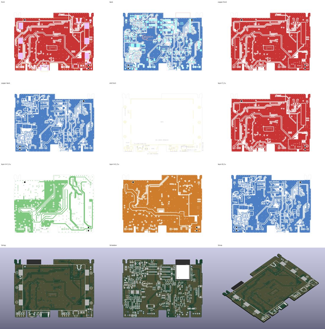
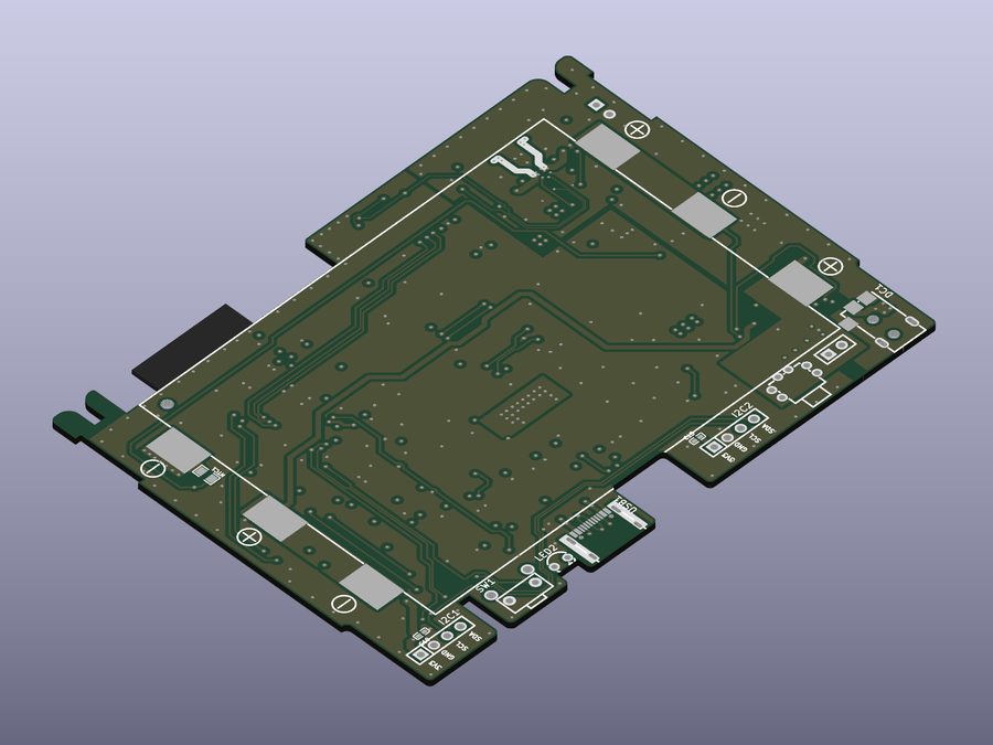
3D, for the things no 2D plot shows — connector orientation, component
collisions, which side is which. --glb additionally writes a board.glb that
GitHub and every browser render interactively:
The schematic, rasterised per sheet plus a real PDF (sheet 1 of 3):
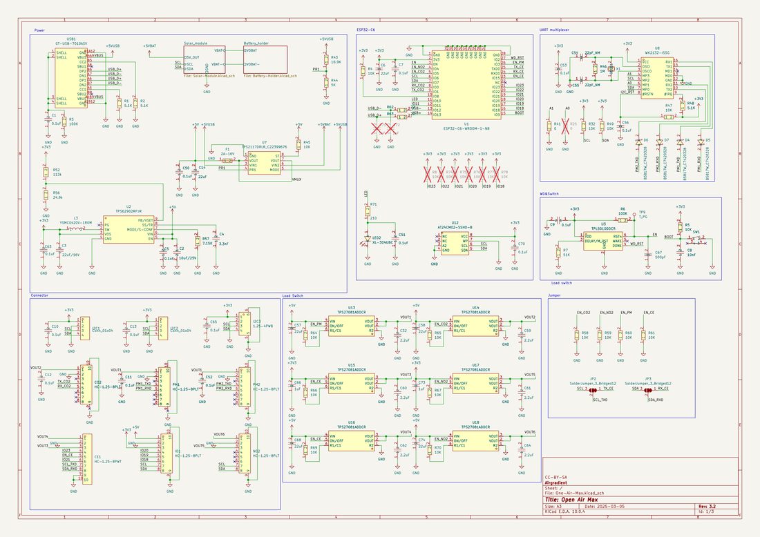
And the verdict, abridged from report.md — note the collapsing: 199
identical drill violations are one line, not 199:
## Verdict
* schematic: 3 error, 19 warning, 4 info
* board: 8 error, 26 warning, 6 info
* 99.45 x 72.0 mm, 4 layers, 210 footprints, 156 nets, 410 vias

## Board findings
| severity | rule | where | message |
| --- | --- | --- | --- |
| error   | `drc.drill_out_of_range` | 199 locations | 199 occurrences. First: Hole size out of range (min hole 0.5080 mm; actual 0.4000 mm) |
| error   | `drc.clearance`          | 13 locations  | 13 occurrences. First: Clearance violation (clearance 0.1000 mm; actual 0.0910 mm) |
| error   | `drc.zones_intersect`    | Zone [BAT-] on F.Cu, priority 5 | Copper zones intersect (must have distinct priorities) |
| warning | `drc.parity.net_conflict`| Pad 6 of I2C3 on B.Cu | Pad net doesn't match net given by schematic (GND) |
| warning | `drc.silk_edge_clearance`| 8 locations   | 8 occurrences. First: Silkscreen clipped by board edge |
Simulation
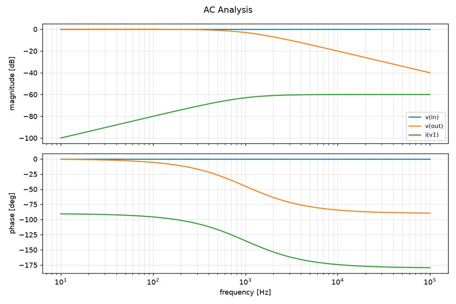
The same “show, don’t describe” applies to analog work. An AC sweep of the RC reference circuit, and 200 Monte Carlo trials of the same circuit with 1 % resistors and 10 % capacitors:
sim run (AC) |
sim montecarlo |
|---|---|
 |
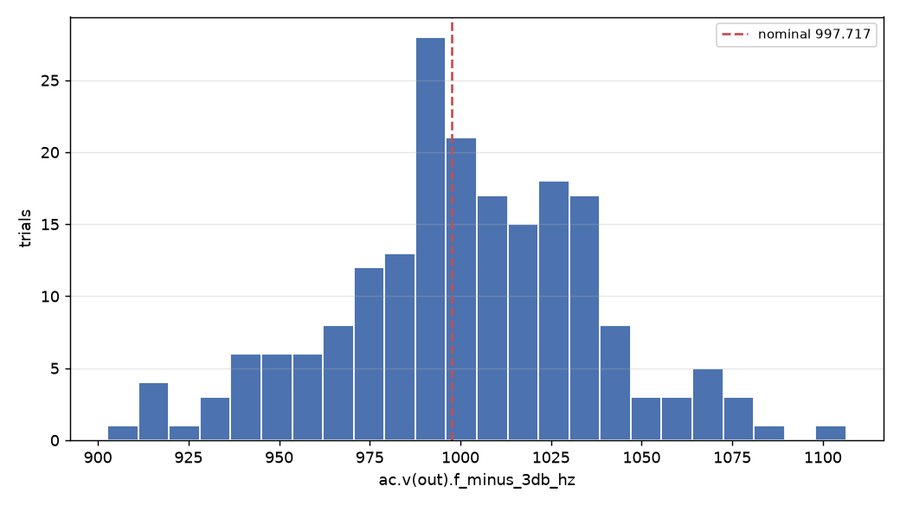 |
{"nominal_metric": 997.7,
 "statistics": {"samples": 200, "mean": 1001.1, "stdev": 35.5,
                "p05": 940.1, "median": 1000.7, "p95": 1064.0, "spread_pct": 20.4}}
The 10 % capacitor sets the spread: ±1 % on the resistor barely moves it. That is the kind of answer that changes a BOM line.
Provenance and licensing of these images: docs/examples/README.md.
Command reference
eda doctor                                    tool versions in the environment
eda gate         TARGET [--policy NAME|FILE] [--text] [--threshold KEY=VALUE]
                        [--collapse N] [-o verdict.json]
eda gate         --list-policies | --list-rules [--text]
eda diff         OLD NEW -o DIR [--dpi 150] [--no-images]
eda report       TARGET -o DIR [--dpi 200] [--glb] [--simulation NETLIST]
                              [--no-3d] [--no-per-layer] [--no-bom] [--title T]

eda datasheet info   PDF
eda datasheet find   PDF QUERY... [--regex]
eda datasheet text   PDF [--pages 1-5] [--layout] [--ocr]
eda datasheet tables PDF [--pages 5]
eda datasheet images PDF -o DIR [--pages]
eda datasheet pages  PDF -o DIR [--pages] [--dpi 200]
eda datasheet parse  PDF -o DIR [--renders] [--ocr]

eda sim lint     NETLIST
eda sim run      NETLIST -o DIR [--no-plots] [--timeout S]
eda sim montecarlo NETLIST -o DIR --vary R1=1% --metric ac.v(out).f_minus_3db_hz [--trials N]
eda sim temperature NETLIST -o DIR [--temperatures -40 25 85] [--metric ...]
eda sim measure  RAW [--thd SIGNAL --fundamental HZ] [--skip S]
eda sim plot     RAW -o DIR [--signals ...]
eda sim netlist  SCHEMATIC -o FILE           export a SPICE deck from KiCad

eda sch info     TARGET [--no-cli]
eda sch review   TARGET [--text] [--collapse N] [--threshold KEY=VALUE] [-o report.json] [--no-cli]
eda sch bom      TARGET -o bom.csv [--group-by ...] [--fields ...]
eda sch erc      TARGET                      raw KiCad ERC JSON
eda sch netlist  TARGET [--format json|kicadxml|spice|...] [-o FILE]
eda sch render   TARGET -o DIR [--dpi 200]   PDF + one PNG per sheet + contact sheet
eda sch pdf      TARGET -o FILE              just the PDF

eda pcb info     TARGET
eda pcb review   TARGET [--text] [--collapse N] [--threshold KEY=VALUE] [-o report.json]
eda pcb fab      TARGET -o DIR [--step] [--ipc2581] [--pos-format csv]
                              [--preview] [--background white|black|transparent]
eda pcb drc      TARGET [--no-parity]        raw KiCad DRC JSON
eda pcb render   TARGET -o DIR [--views ...] [--per-layer] [--no-3d] [--no-sheet]
                              [--glb] [--dpi 300]
                              [--background white|black|transparent]
eda pcb glb      TARGET -o FILE              3D model a browser can display
eda pcb electrical TARGET [--temperature-rise K] [--top N] [--solve]
eda pcb crosstalk TARGET [--rise-ns NS] [--swing V] [--min-coupled MM] [--limit N]
                              [-o DIR]
eda pcb thermal  TARGET --power REF=W [--power ...] [--ambient C] [--htc W_M2K]
                              [--step MM] [--transient S] [-o DIR]
eda pcb stats    TARGET
TARGET accepts a .kicad_sch/.kicad_pcb file, a .kicad_pro, or a project
directory. All commands print JSON by default (the review commands also take
--text for a human readable digest) and exit 2 when a review found errors.
Environment variables
| Variable | Effect |
|---|---|
KICAD_VERSION |
KiCad release / image tag to use (default 10.0.4) |
EDA_IMAGE |
override the image name entirely |
EDA_NETWORK |
1 gives the container network access (default: offline) |
EDA_MOUNT |
host directory to mount at /work (default: git root or $PWD) |
EDA_ENV_PASSTHROUGH |
extra environment variable names to forward |
EDA_DOCKER_ARGS |
extra arguments for docker run |
Using it in CI
The reviews are exit-code gates, so a board can be checked on every push the way code is. In a project that added this as a submodule:
# .github/workflows/hardware.yml
- uses: actions/checkout@... # with: submodules: true
- name: Gate the design
  run: ./bin/eda.sh gate hardware/ --policy hardware/gate.toml --text
- name: Review the board
  if: always()
  run: |
    ./bin/eda.sh sch review hardware/ --text
    ./bin/eda.sh pcb review hardware/ --text
- name: Build the report
  if: always()
  run: ./bin/eda.sh report hardware/ -o build/report
- uses: actions/upload-artifact@...
  if: always()
  with: { name: hardware-report, path: build/report }
On a pull request the more useful question is what changed. eda diff answers it
against the design rather than the file: a moved component rewrites thousands of
coordinates in the .kicad_pcb, and a text diff cannot tell that apart from a
rerouted net.
- name: What changed
  run: |
    git worktree add /tmp/base "$GITHUB_BASE_REF"
    ./bin/eda.sh diff /tmp/base/hardware hardware/ -o build/diff
    cat build/diff/diff.md >> "$GITHUB_STEP_SUMMARY"
## Connectivity
* **VCC**: gained U3.14, lost -
## Components
* **R7**: value '10k' -> '4k7'
## Board
* moved: U3 (5.0 mm), C12 (1.2 mm)
## Artwork
* `copper-front`: 0.28% of pixels changed
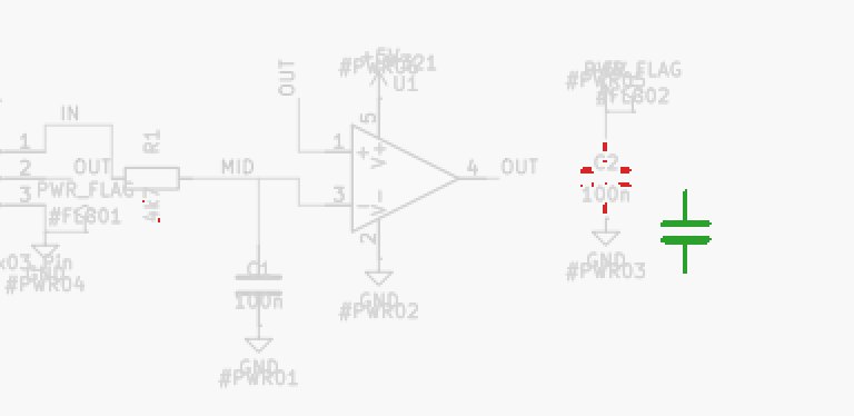
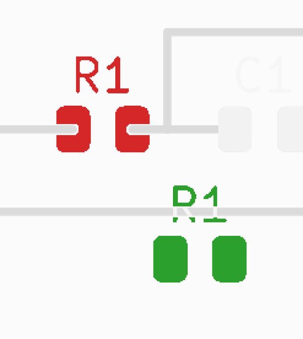
Both drawings are rendered and compared too — the schematic sheets and the board plots. What only the old revision had is drawn in red, what only the new one has in green, over a faded copy of the new drawing, so a part that moved reads as red where it was and green where it is now. Where the change is a speck on an A4 sheet, a zoomed crop is written alongside the full page:
| schematic: C2 moved, R1 re-valued | board: the same R1 move |
|---|---|
 |
 |
Exit 0 clean, 1 on a usage error, 2 when a review found errors. Loosen or
tighten what counts as an error with --threshold KEY=VALUE, or post-process
report.json if you want your own policy. This repository’s own CI reviews its test
fixture and uploads the report the same way — see
ci.yml.
Nothing needs the network at run time, so the container stays offline unless you
ask for EDA_NETWORK=1.
Using it with a coding assistant
The toolkit is a CLI: any assistant that can run a shell command can drive it,
and the JSON output is meant to be parsed rather than screen-scraped. What makes
the difference in practice is not the commands but knowing how to use them —
which is what docs/guides/ is for. Those guides cover
the review methodology, what each finding means, and what the tool cannot judge
for you.
- Codex and Agent Skills-compatible assistants discover
.agents/skills/<name>/SKILL.md. - Claude Code discovers
.claude/skills/<name>/SKILL.md. bin/install-skills.shcreates both layouts as symlinks by default. Run it in this checkout or in a project that uses the submodule. This checkout ignores the generated adapters; a parent project must ignore or track its own copies.- A tool with another layout — use
./bin/install-skills.sh --dest .cursor/rules --copy; specifying--destinstalls only that layout. - Anything that reads a repository can instead read
docs/guides/orAGENTS.md, which names the guides. - No assistant at all — they are ordinary Markdown, written to be read.
Contributor and agent instructions for this repository itself live in
AGENTS.md (CLAUDE.md is a pointer to it, not a second copy).
eda gate is the other half of that story. An assistant that generates a
design will read a page of warnings and move on unless something says which of
them were allowed to survive; the gate is that statement, and its exit code is
the loop condition. The design gate guide
describes the generate → gate → fix loop.
eda report exists largely for this use case: an assistant working headlessly
can produce one page — renders, findings, BOM, simulation plots — that a human
can check at a glance instead of taking a summary on trust.
How it fits together
bin/eda.sh            host wrapper: docker run, uid mapping, network policy, path rewriting
bin/install-skills.sh CLI shim + renders docs/guides/ into an assistant's layout
docker/Dockerfile     kicad/kicad:<version> + ngspice + an isolated virtualenv
src/eda_toolkit/
├── cli.py                 the `eda` command
├── gate.py                policies, waivers, and the one pass/fail verdict
├── report.py              the one-command report: collect, then render md/html
├── datasheet/             PDF text, table, image and page extraction
├── spice/                 ngspice runner, raw-file parser, measurements, plots
└── kicad/                 s-expression parser, schematic/board models,
                           outline geometry, kicad-cli wrapper, review rules,
                           renderers, fabrication package
tests/                     pytest suite + fixtures + smoke test
docs/guides/               the usage guides - prose, and the source of truth
docs/examples/             committed output, so the README shows rather than tells
AGENTS.md                  contributor / agent instructions (CLAUDE.md points here)
Design notes:
- KiCad is the source of truth where it can be: ERC, DRC, netlist export
and plotting all go through
kicad-cli. The hand-written parsers add what the CLI does not expose (geometry, stackup, pad positions, properties) and provide a pure-python fallback so the library, and the test-suite, still work without KiCad installed. - Review = rules + pictures. The rule engine produces structured findings;
the renderers produce PNGs so the parts a rule cannot judge (placement,
routing quality, silkscreen legibility, signal flow) can be looked at. This
matters most when the work is headless:
eda reportexists so whoever is driving - a person on a CI artifact, or an assistant mid-task - can see the design instead of taking a JSON summary on faith. - Geometry is measured, not approximated. Board-edge clearance is computed against the flattened Edge.Cuts geometry, arcs and circles included, with an inside/outside test that survives cutouts and the seams where two outlines meet. A bounding box gets a round board, a notch or a mounting hole wrong in both directions.
- Findings are typed (
rule,severity,message,location,details) and every rule is a small function registered in a list — adding a check is a dozen lines plus a test. - The knowledge is in Markdown, not in prompts. The judgement calls that make
a review useful live in
docs/guides/as prose, so they are reviewable in a diff and usable by a person, a script or any assistant. One tool’s directory layout is generated from them, never the other way round.
Review quality
The rules were tuned by running them over the 18 KiCad demo projects that ship
with the image (/usr/share/kicad/demos), which is a far harsher corpus than
the test fixture. That pass produced three fixes:
- KiCad’s global library tables are now seeded from Python, not only by the container entrypoint. Without them every symbol reports “the current configuration does not include the library …”, which was 1965 findings of pure noise across the corpus.
- Power symbols are recognised by KiCad’s real invariant - the
#reference prefix - not just by apower:library id. Older projects were reporting every GND symbol as a component with no footprint. net.single_pinis graded by whether the net was named by the designer, and any rule that fires more than six times is folded into one finding with a count. Oninterf_uthe review went from 113 warnings to 2.
Re-run it after changing a rule:
docker run --rm -v "$PWD:/work" -w /work -e PYTHONPATH=/work/src \
  --entrypoint python3 eda-toolkit:10.0.4 tools/review_demos.py /tmp/out
Reproducibility
Every external input is pinned, and the pins are enforced by
tests/test_pinning.py (which runs in CI):
| Input | Pin |
|---|---|
| KiCad base image | manifest digest, per version, in docker/kicad-digests.txt |
| pip / uv | exact version + wheel SHA-256 (ARG PIP_*, docker/uv-bootstrap.txt) |
| Build backend | exact version in [build-system] requires + wheel SHA-256 in docker/build-backend.txt — uv.lock cannot cover it, so the image installs it separately and builds with --no-build-isolation-package |
| Python packages | uv.lock - exact versions + artifact hashes for the whole tree, installed with uv sync --frozen |
| GitHub Actions | 40 character commit SHA, with the tag in a trailing comment |
| CI runner | ubuntu-24.04, never -latest; Python 3.13.5 |
Keeping them current:
- Dependabot (
.github/dependabot.yml) opens weekly PRs foruv.lockand the actions. make check-pins(and the manually dispatchedpins.ymlworkflow) covers what Dependabot cannot parse: the KiCad image digest and the pip/uv bootstrap wheels. When upstream moved, the workflow pushes the update toautomation/refresh-pinsand links to the PR creation page in its run summary — opening the PR stays a human act. The default KiCad release is never bumped automatically.
To change a dependency, edit pyproject.toml and regenerate the lock:
make lock          # uv lock
make rebuild
To use another KiCad release, add its digest to docker/kicad-digests.txt
(the file documents the one-liner) and build with KICAD_VERSION=<version>.
The build fails loudly if a version has no pinned digest.
Testing
make test          # everything, inside the container
make test-coverage # the same, with a coverage report
make test-host     # pure-python subset on the host (needs a local venv)
make lint          # ruff
make smoke         # end-to-end: every top-level command
make skills        # mirror guides into .agents/skills and .claude/skills
make site          # render the GitHub Pages site into _site/
CI (.github/workflows/ci.yml) runs on every push
and pull request:
| Job | What it proves |
|---|---|
unit |
ruff (lint + format) and the pure-python suite against the hash-pinned dependency set |
container (KiCad 10.0.4) |
the full suite, coverage and the smoke test inside the freshly built image |
container (KiCad 9.0.9) |
the same, one KiCad major behind - the toolkit really is version-portable |
Both container jobs upload eda report output for the example project, so every
run leaves behind a page you can look at. Nothing in CI touches the network
beyond pulling the pinned base image and the locked wheels.
The suite covers the s-expression parser, schematic and board models, the
outline geometry (arcs, circles, cutouts, seams), every review rule, the
report renderers, the submodule installer, the ngspice raw-file parser
(ASCII/binary, real/complex), the
measurement maths (checked against analytically known circuits), the datasheet
PDF extraction (against a generated PDF), and the CLI. Tests that
need kicad-cli or ngspice are marked and skipped automatically outside the
container.
Integration tests run the real tools: KiCad ERC and DRC on the example project,
a deliberately introduced short to prove DRC catches it, netlist comparison
between kicad-cli and the fallback extractor, layer/3D rendering, and an RC
filter whose simulated −3 dB corner is compared against 1/(2πRC).
Limitations
- Getting datasheet PDFs is out of scope - the container has no network. Save the PDF into the repository first, then parse it.
- Embedded-image extraction only recovers raster images. Most datasheet figures
are vector art — render the page instead (
datasheet pages). sim netlist(KiCad → SPICE) only produces a usable deck when the schematic carries Spice model fields.- The review rules encode common practice, not your fab’s or your project’s
rules. Thresholds are adjustable (
--threshold); the defaults are conservative low-cost-fab values. - OCR of scanned datasheets needs
tesseract, installed only if a Debian mirror is reachable at build time (WITH_OCR=0to skip). Everything else works without it.